P6 Micro-Ops: Decode, Flags, Control Flow, and Macro Aliasing
In the earlier z386 and z486 posts, we watched Intel's 32-bit x86 designs evolve from a microcoded state machine with early-start overlap (386) into a tightly coupled 5-stage pipeline (486). Even on the dual-pipe Pentium (1993), what flowed down the pipeline was still recognizably an x86 instruction: decode logic resolved prefixes and addressing modes, walked the instruction through an in-order datapath, and retired results in lockstep.
With the P6 microarchitecture, introduced in the Pentium Pro (1995) and carried forward through Pentium II, Pentium III, and Pentium M, Intel changed things dramatically. Externally, a P6 chip still runs raw 16- and 32-bit IA-32 binaries. Internally, x86 instructions cease to exist after the decoder. Every instruction is translated into P6's private RISC-like instruction set: micro-operations (µops).
doom1.wad, shown at 10× speed) on p6.c—a sequential C simulator of P6 micro-ops.As with the earlier 386 and 486 posts, this series looks at the P6 microarchitecture through CPU internals and microcode—µops in this case. Most textbook accounts jump straight from "x86 decodes into µops" to Tomasulo register renaming, Reservation Stations, and Reorder Buffers; here we will focus on concrete microcode examples and RTL design.
As the DOOM run above demonstrates, P6's µop layer is a complete, self-contained execution architecture in its own right. It sits between the x86 architecture layer and the underlying out-of-order machine. And I think it is an important historical piece of technology to understand.
Community Work on Understanding P6
During the past few months, I've built on existing community reverse-engineering efforts on Intel's P6 microcode architecture:
- Peter Bosch (
peterbjornx): In 2020, Peter pioneered P6 microcode reverse engineering using a metallographic microscope—breaking the P6 microcode update format, 3-slot triad bit-scrambling, and internalCRBUSaccess, and releasingp6tools(uc_isa.py,descramble.py,simpledis.py,simpleas.py) along with patch utilities (patchtools, without key material). His tweets and writeup ended with a classic nerd-snipe: "Yep. If anyone wants to mess around with microcode, a lot of the tools are on github. Some assembly required but you should be able to get it to work." (Feb 12, 2021) - Rudolf Marek (
ruik): Picked up that challenge around April 2025, reproducing Peter's work to achieve arbitrary microcode execution on a Pentium II (Dixon), then extendingpatchtools_pubandutools(alongsidemicrocode-patch-collection) with key material and ROM dumpers across Pentium Pro, Pentium II, Pentium III, Pentium M, and first-generation Intel Core processors—making it practical to dump internal ROMs, build accepted patches, and run custom microcode from Linux usermode or DOS. - Martin Hinner: Joined Rudolf in August 2025, greatly extending the assembler, disassembler, and scrambler (
p6microcode-tools) while spending extensive effort on cross-CPU analysis and on-hardware verification across P6-family processors, and creating the P6 Microcode Wiki, cataloguing P6µopmnemonics (such asTRANSPORTUIP,WUINSERT, andSIGEVENT), logical register tables,CRBUSregisters, and cross-stepping notes. He is also documenting AMD microcode and welcomes collaborators interested in helping extract AMDMSROM. (Whilep6microcode-toolsis not yet publicly released, Rudolf and Martin are happy to share it with anyone interested in collaborating on P6 microcode reverse engineering.)
Intel's large body of P6-era patents was also very helpful—especially patents US5721855, US5559974, US5627985, US5574871, US5680565, and their companions (listed in the references).
From there, the main way forward was live Pentium Pro hardware experiments. Nothing beats real hardware tests for settling ambiguities. The existence of the P6 microcode patching mechanism means I could change the microcode in any way I wanted—something not possible on the 386 or 486. So over 200 targeted microcode and architectural probes were built and executed on a physical Pentium Pro (CPUID 0619h, stepping 9) testbench to resolve undocumented field encodings and verify P6-specific behavior (unless noted otherwise, all MSROM excerpts and hardware measurements below come from this CPUID 0619h Pentium Pro). That turned out to be fruitful: my understanding of P6 µops is now complete enough to write p6.c, a µop-based simulator that boots DOS and runs DOOM.
Quick View of a P6 Die
Before zooming into individual µop bits, it helps to look at an actual P6 die to see two things at once: where Intel spent its transistor budget (5.5 million transistors on the original Pentium Pro core die, growing to 7.5 million on Pentium II with larger L1 caches and MMX), and which blocks sit next to each other because neighboring units communicate over tight, timing-critical wires:
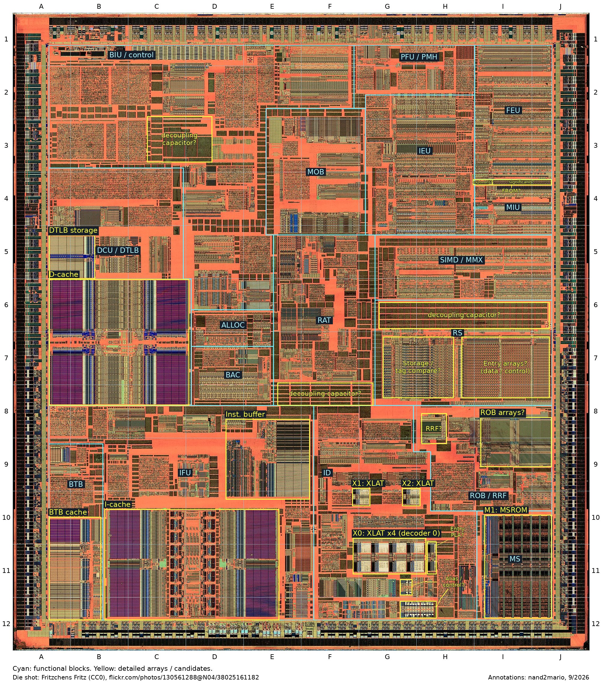
Base photograph: Fritzchens Fritz (CC0).
(Note on chip generation: this photograph shows a 250 nm Pentium II (Deschutes) rather than the 350 nm Pentium Pro (CPUID 0619h) from which my ROM dumps come—for example, the SIMD / MMX block at G5–I5 was added after Pentium Pro. Even so, Pentium II uses the same core P6 microarchitecture, making its floorplan an illuminating map of the machine.)
At a quick glimpse, P6 is a world apart from the 1.2-million-transistor i486 we studied in z486. On an i486 die, outside the 8 KB unified cache and x87 FPU, almost everything is a linear in-order datapath: a compact D1/D2 decoder cracks one instruction at a time and drives the address adder, ALU, and microcode ROM in lockstep. On P6, by contrast, the actual arithmetic hardware occupies only a modest corner—most of the non-cache silicon goes into decoupling variable-length x86 instructions from out-of-order execution:
- Fetch & Branch Prediction (
A7–E12, bottom-left): The Instruction Fetch Unit (IFU,C9) sits wedged directly between the Branch Target Buffer (BTB,A9–B12), L1I-cache(B10–E12),Inst. buffer(D8–E9), and Branch Address Calculator (BAC,D7), keeping predicted target steering and 16-byte instruction-block fetches on short local wires before aligned x86 bytes cross rightward intoID. - x86-to-
µopTranslation & Microcode (F8–J12, bottom-right — our focus in this post): Notice how much silicon P6 spends purely translating x86 bytes intoµops. InsideID(F8–H12), you can spot the asymmetric 4 + 1 + 1 decoderXLATPLA candidates: four side-by-side PLAs atX0: XLAT x4(G10–H11, general decoderD0) and two single-µopPLAs above them atX1andX2(G9–H9, simple decodersD1andD2). Their immediate neighbors tell the rest of the story:- Directly touching
X0's right edge atH10sits theEntry PLA?candidate—matching patentUS5559974Figure 5, whereXLATand the entry-point PLA share the same opcode inputs while the entry PLA steersM1: MSROMright next door (I10–J12). - Directly below
X0(G11–H12) sit twoAlias / control?array candidates, positioned right whereµoptemplates from bothXLATandMSROMconverge to be specialized with decoded instruction fields before heading north.
- Directly touching
- Out-of-Order Bookkeeping Across the Center (
D6–J9): The entire middle band of the chip isn't arithmetic at all—it is dynamic-execution bookkeeping:ALLOC(D6),RATregister renaming (E6–F7), the 20-entry Reservation Station (RS,G6–J7), and the 40-entry Reorder Buffer and committed register file (ROB / RRF,H8–J9), bridging the bottom front end (3 µops/cycle) upward to the execution units. - Compact Execution Units (
G2–J5, top-right): Compared to caches, decode, and scheduling, the actual math units—integerIEU(G2–H4) and floating-pointFEU(I2–J3, with the thinFROM?floating-point constant ROM candidate alongI4's upper edge)—take up surprisingly modest area right aboveRSandROB / RRF. - Memory Ordering & Data Cache (
A1–F8, upper-left): The Memory Order Buffer (MOB,E2–F4) sits at the crossroads betweenDCU / DTLBand L1D-cache(A5–C8) on its left and the core execution engine to its southeast, tracking in-flight loads and stores before memory updates reach the cache.
So here we go. Let's head into the bottom-right corner of the die—ID and MSROM—and see how x86 instructions become µops.
1. Translating Variable-Length x86 into Fixed µops (XLAT vs. MSROM)
Why not execute x86 instructions directly, the way the 486 and Pentium did?
Consider three ordinary IA-32 instructions sitting back-to-back in a loop:
03 44 8B 08    add eax, [ebx + ecx*4 + 8]   ; 4 bytes: memory load + 32-bit ALU add + EFLAGS
49             dec ecx                      ; 1 byte:  subtract 1, update 5 flags (keep CF!)
75 F9          jnz .loop                    ; 2 bytes: test ZF and redirect EIP
Directly pipelining instructions like these gets painful fast:
- Variable length (1 to 15 bytes): You don't know where instruction #2 starts until you have parsed all prefixes, opcode bytes,
ModR/M,SIB, displacement, and immediate bytes of instruction #1. - Compound memory-plus-ALU work:
add eax, [ebx + ecx*4 + 8]computes a scaled address, checks segment limits and page permissions, reads 4 bytes from cache, adds them toEAX, and updates six status flags. Meanwhileadd [ebx], eaxreads memory, modifies the value, and writes memory back. - Asymmetric operand rules: Registers can be 8-bit (
AL,AH), 16-bit (AX), or 32-bit (EAX), implicit (ESPinPUSH,ECXinLOOP,EDX:EAXinMUL) or explicit.
P6's front end solves this by translating every x86 instruction into one or more 72-bit µop templates that always follow a uniform RISC-like discipline: at most two source registers, one destination register, and strictly separated memory loads, ALU operations, and memory stores. (Following Intel's decoder patent US5559974, a raw 72-bit template from the decoder PLAs or ROM—still carrying alias control bits—is called a Cuop, and once instruction-specific fields are substituted in, the resolved operation is called an Auop.)
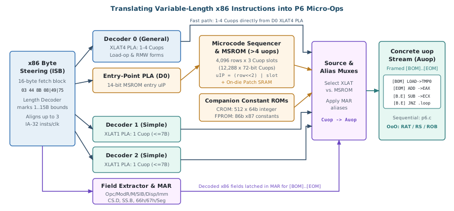
XLAT), 3-slot MSROM triads, and the Macro-Alias Register (MAR) muxes into a uniform [BOM]..[EOM] µop stream.As shown above, P6 splits x86-to-µop translation across two hardware sources using an asymmetric 4-1-1 decoder layout (patent US5630083; Shen & Lipasti §7.3.3):
- Simple Decoders
D1andD2(1 µopeach): Rather than paying the silicon area of three full x86 decoders,D1andD2only handle common, prefix-light instructions (≤ 7 bytes) that turn into a singleCuop—register-to-register math (DEC ECX), register loads (MOV EAX, [EBP+8]),LEA, and simple conditional jumps (JNZ). - General Decoder
D0(XLAT4,1to4 µops):D0's combinational translation PLA (XLAT4) handles any x86 instruction up to 4Cuops in a single clock—such as our 2-µopADD EAX, [EBX + ECX*4 + 8](LOAD+ADD), a 3-µopPUSH EAX, or a 4-µopread-modify-writeADD [mem], EAX. (If a multi-µopinstruction happens to land onD1orD2, hardware simply holds it forD0on the next cycle.) - The Microcode Sequencer and
MSROM(> 4 µops): WhenD0sees a complex instruction—anything fromCPUID,CMPXCHG,ENTER, andREP MOVSup toIRETand x87 transcendentals likeFSIN—D0hands a 14-bit starting microaddress (µIP) to the Microcode Sequencer (MS), which fetches 72-bitCuops from the on-die Microcode Sequencer ROM (MSROM).
Every x86 instruction takes one of three paths through D0 and MSROM:
- Pure
XLAT(1–4µops): Over 90% of dynamic instructions in typical integer programs (and in the DOOM run above) finish right insideD0/D1/D2without ever touchingMSROM. - Hybrid
XLAT4Prefix +MSROMContinuation: To avoid wasting a cycle whileMSROMis read,D0can emit up to four setupCuops fromXLAT4on cycletwhileMSROMseamlessly continues emitting the rest of the routine on cyclet + 1. MSROM-Only: Rare or serializing instructions (CPUID,LGDT,HLT,LOCKread-modify-write forms) jump straight to anMSROMentry point.
Anatomy of a 72-Bit Cuop
Let's look at what sits inside one 72-bit Cuop coming out of XLAT or MSROM—and how MSROM packs them into physical rows. (Note: this reflects our current working layout for Pentium Pro CPUID 0619h, matching the P6 Microcode Wiki uops reference. Several bitfields—particularly the upper bits of U2 and certain field combinations—are still work-in-progress / TBD, and community contributions are very welcome! Throughout the rest of this post, blue highlights 72-bit Cuop fields and bit slices, while amber highlights actual 0619h MSROM addresses.)
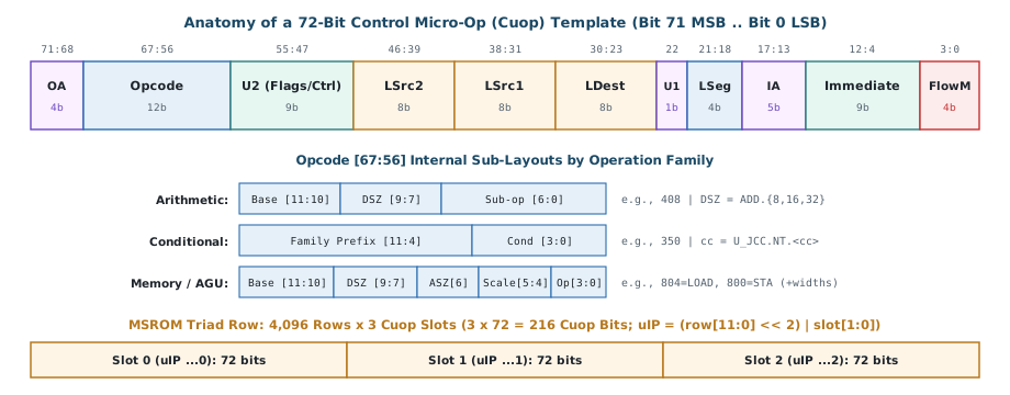
µop (Cuop). Middle: How the 12-bit Opcode encodes width, condition, or scale sub-fields by family. Bottom: Each MSROM triad row holds three 72-bit Cuop slots (...0, ...1, ...2).Even though 72 bits is wider than a 32-bit MIPS or RISC-V instruction, the 11 fields break down into five clean roles that we will meet throughout this post (the community names U1 and U2—originally "unknown" control fields—are kept here for consistency with existing P6 microcode tools):
- What to do (
Opcode [67:56], 12 bits): Selects the execution primitive (ADD,LOAD,STA,U_JCC, ...) together with family-specific sub-fields for data width (DSZ), address width (ASZ), SIB scale (Scale), or branch condition (Cond). - Flag & modifier profile (
U2 [55:47], 9 bits): Operation-dependent control bits—most importantlyU2[4:0], which selects which architecturalEFLAGSbits (if any) an integerµopis allowed to overwrite (Section 2), while upper bitsU2[8:5]and non-integer profiles carry additional controls (several still TBD). - Three register operands + segment (
LSrc2 [46:39],LSrc1 [38:31],LDest [30:23]at 8 bits each;LSeg [21:18], 4 bits): Name up to two source registers, one destination register (architectural registers likeEAX, internal scratch registersTMP0–TMPE, or discard targetSINK), and the memory segment (DS,SS,ES, ...). - Immediate & constant steering (
Immediate [12:4], 9 bits +IA [17:13], 5 bits):IA(ImmAlias) steers the 9-bitImmediatefield—selecting an inline signed literal (#n), a decoded x86 displacement/immediate, a 64-bit Constant ROM (CROM) entry, or even a 14-bit microbranch address(LSrc2<< 9) |Immediate(Section 3). - Template alias switches & framing (
OA [71:68], 4 bits +U1 [22], 1 bit;FlowM [3:0], 4 bits):OA(OpAlias),U1,IA, and the upper bits of the operand fields let a single staticCuopact as a generic hardware template across operand widths and decoded x86 registers (Section 4), whileFlowMframes x86 instruction boundaries.
Physical packing and an address quirk: Notice the bottom bar of the diagram as well. Because P6's core issues up to three µops per cycle, both MSROM and the patchable MSRAM physically pack each triad of three 72-bit Cuops into 7 × 32-bit words—and the bits are heavily scrambled across two transformations (MSROM → MSRAM → logical Cuop). On the addressing side, MSROM holds 4,096 triad rows, and P6's 14-bit µIP wire and branch-target encoding is bit-sliced into (row[11:0] << 2) | slot[1:0] (allowing micro-branches to target mid-triad slots ...1 and ...2 as well as ...0). That is why hardware µIPs in the MSROM disassembly count ...0, ...1, ...2, ...4, ...5, ...6, skipping every fourth hex address (...3, ...7, ...B, ...F).
Keeping x86 Instructions Whole: [BOM] and [EOM]
Once a 4-µop ADD [mem], EAX or a 30-µop ENTER cracks into individual µops, how does the CPU remember where one x86 macroinstruction begins and ends? That is the job of the 4-bit FlowM [3:0] field at the right end of every Cuop:
[BOM](Beginning of Macroinstruction): Marks the firstµopof an x86 instruction.[EOM](End of Macroinstruction): Marks the finalµopof an x86 instruction. Only when[EOM]finishes does architecturalEIPadvance to the next x86 instruction, and only between[EOM]and the next[BOM]can ordinary external interrupts (INTR) or single-step traps (TF) fire.[BOM.EOM]: Both bits set—a single-µopx86 instruction such asDEC ECXorADD EAX, EBX.
In my sequential p6.c simulator, executing one x86 instruction is as simple as fetching Cuops from [BOM] through [EOM], specializing any aliases into concrete Auops, and updating architectural state cleanly when [EOM] completes.
2. Arithmetic, Flags, and Split Memory Ops
Now let's look at the µops themselves. What primitives do XLAT and MSROM use to compute integer results, manage x86's notoriously finicky EFLAGS, and read or write memory?
2.1 Scratch Registers (TMP0–TMPE) and Load-Operate
Suppose P6 decodes add eax, [ebx + ecx*4 + 8]. An ALU µop cannot read memory directly, so D0's XLAT4 cracks the instruction into two µops using one of P6's 15 named scratch registers (TMP0–TMPE in hex, plus discard target SINK). (Interestingly, the exact physical bit widths of individual TMP registers—which ones are strictly 32-bit vs. wider 64/86-bit for floating-point packets—are still partially unknown and under active hardware investigation.)
; Conceptual resolved Auop pair for: add eax, [ebx + ecx*4 + 8]
[BOM] TMP0 := LOAD.ASZ32.SC4.DSZ32(ECX, EBX, +0x08, SEG_DS) ; LSrc1 = scaled index (ECX*4), LSrc2 = base (EBX)
[EOM] EAX  := ADD.DSZ32(EAX, TMP0, FLAGS_ALL)
Notice the clean division of labor:
LOADcomputesEBX + ECX * 4 + 8inside the Load Address Generation Unit, verifiesDSsegment limits and page read permissions, and places the 32-bit value from memory intoTMP0.ADD.DSZ32addsEAX + TMP0, writesEAX, and updates all six architectural arithmetic flags (CF, PF, AF, ZF, SF, OF).
What if the destination is memory instead—add dword ptr [ebx + ecx*4 + 8], eax? Now D0 emits a 4-µop read-modify-write sequence:
; Conceptual resolved 4-uop flow for: add [ebx + ecx*4 + 8], eax
[BOM] TMP0 := LOAD.ASZ32.SC4.DSZ32(ECX, EBX, +0x08, SEG_DS)
      TMP0 := ADD.DSZ32(TMP0, EAX, FLAGS_ALL)
      STRD.DSZ32(ZERO_VAL, TMP0)
[EOM] STA.ASZ32.SC4.DSZ32(ECX, EBX, +0x08, SEG_DS)
Look at the last two lines—every memory store in P6 is split into two separate µops:
STRD(Store Data): Captures the value to be written in its second source slot (TMP0; its unused first source reads P6's hardwired zero operandZERO_VAL).STA(Store Address): Computes the target address (EBX + ECX*4 + 8) and validates segment and page write permissions (#GP,#SS,#PF).
Even a humble push ebp is three µops (STRD to supply EBP, STA to write [ESP - 4], and SUB to decrement ESP by 4). In a sequential simulator like p6.c, splitting a store into STRD + STA looks like wasting cycles. In P6's out-of-order core, this actually helps performance. It lets hardware compute a store's address early, so younger loads immediately know whether they overlap that address while the store's data is still being calculated.
2.2 P6's Two-Tier Flag Model: Per-Register Flags vs. EFLAGS
While building z386 and z486, I ran into two recurring headaches caused by EFLAGS:
- Microcode scratch math must never clobber user
EFLAGS: An instruction likeIN EAX, DXorLGDT [EBX]is defined by Intel's manual to leaveEFLAGScompletely unchanged. Yet insideMSROM,IN EAX, DXhas to shift port numbers, mask I/O permission bits, compareCPLagainstIOPL, and branch on the results. If internalSUBandANDµops overwroteEFLAGS, microcode would constantly corrupt the running program's flags. - Partial flag updates:
ADDandSUBupdate all six arithmetic flags (CF, PF, AF, ZF, SF, OF),INCandDECupdate five flags while preservingCF,MULupdatesCFandOF, andBTSupdates onlyCF.
When I first disassembled the MSROM, lines like 0C0A–0C0C looked baffling at first glance:
0C0A: TMP9 := BTEST.DSZ32(TMP9, #20)         ; U2 = 0 (no architectural flags!)
0C0C: U_JCC.NT.NC(TMP9, 11A0, IA_UADDR)      ; Branch to 11A0 if Carry Clear... on TMP9?!
Look closely at 0C0C: U_JCC does not read EFLAGS—it passes TMP9 (written by BTEST) as an explicit source operand and branches on TMP9's Carry flag, while architectural EFLAGS.CF stays completely untouched.
How does TMP9 "have" a Carry flag? Intel's P6 execution-unit patent (patent US5574942, Column 4 & Figure 4a) explains the layout directly: in P6, every internal integer register and operand bus carries a 32-bit data field paired with a per-register Flags field (OF, SF, ZF, AF, PF, CF) holding the flags produced by the last operation that wrote that register (and 86-bit floating-point registers similarly carry a 6-bit FP condition-code field in Figure 4b). In P6's out-of-order hardware, the Reorder Buffer (ROB) entry also stores Data + Flags side by side (patent US5627985 Figure 4).
That gives P6 a clean two-tier flag architecture:
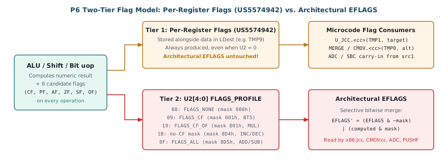
µop writes six per-register flags alongside its destination value (Tier 1, patent US5574942 Fig. 4a), while U2[4:0] selectively merges the desired subset into architectural EFLAGS (Tier 2).- Tier 1 — Per-Register Flags (always produced): Every ALU, shift, or bit-test
µopwrites the six flags it just computed directly into its destination register'sFlagsfield (LDest, such asTMP9). Microcode branches (U_JCC), conditional moves (CMOV), and carry-chained operations read those flags straight off theirLSrc1source register (patentUS5574942Col. 4). By default (U2= 0,FLAGS_NONE), nothing touches architecturalEFLAGS—microcode can subtract, test bits, and branch across multipleTMPregisters in complete isolation. - Tier 2 — Masked Architectural Publication (
U2[4:0]): When an integer operation is supposed to update programmer-visible x86EFLAGS, itsCuopsets an encoded 5-bitFLAGS_PROFILEindex inU2[4:0](not a direct bitwise mask—hardware decodes the 5-bit code into an architecturalEFLAGSbitmask, matching patentUS6047369Fig. 15C/17, and verified across all 32U2[4:0]values on0619hhardware) and merges only the selected bits intoEFLAGS:U2= 00h(FLAGS_NONE,EFLAGSmask000h): per-register flags only (LEA,MOV,NOT, all internal microcode scratch work).U2= 09h(FLAGS_CF,EFLAGSmask001h): updatesCFonly (BTS,BTR,BTC,CLC,STC).U2= 19h(FLAGS_CF_OF,EFLAGSmask801h): updatesCF, OF(MUL,IMUL, 1-bitROL/ROR).U2= 1Bh(FLAGS_PF_AF_ZF_SF_OF,EFLAGSmask8D4h): updatesPF, AF, ZF, SF, OFwhile keeping oldCF(INC,DEC).U2= 0Fh(FLAGS_ALL,EFLAGSmask8D5h): updates all six arithmetic flags (ADD,SUB,CMP,AND,OR,XOR,NEG).
(In the disassembly listings below, raw or operation-specific 9-bit U2 codes without a symbolic alias print in hex as U2.<hex>, such as U2.1B on INC/DEC or U2.21 on MOVEMERGEFLGS.)
What about ADC EAX, EBX (Add with Carry), which needs to read the architectural EFLAGS.CF bit produced by an earlier x86 instruction? As patent US5574942 Column 4 notes, ADC takes its carry-in from the Flags field of its first source operand—so P6 bridges Tier 2 back into Tier 1 with an explicit flag-merge primitive, MOVEMERGEFLGS (seen directly in the MSROM disassembly at 2518–2519 for LOCK ADC, and mirrored in p6.c's authored 2-µop XLAT template matching Intel AP-526's 2-µop count):
; Authored 2-uop XLAT flow in p6.c (matching AP-526 & MSROM @ 2518-2519): ADC @REG_ddd, @REG_sss
[BOM] TMP0     := MOVEMERGEFLGS(ArithFLAGS, @REG_ddd, U2.21)        ; attach EFLAGS.CF onto @REG_ddd's value
[EOM] @REG_ddd := ALU.@MGRP0.@DSZ(TMP0, @REG_sss, FLAGS_ALL)        ; ADC consumes TMP0's CF & updates EFLAGS
(Don't worry yet about template markers like @REG_ddd, @REG_sss, EAX_OPSZ, or .@DSZ in these listings—for now just read @ as "substituted from the decoded x86 instruction"; Section 4 explains them.)
2.3 Branchless Microcode Idioms: CMPXCHG Without a Jump
Per-register flags unlock another neat trick: branchless microcode.
Consider CMPXCHG r/m, r (Compare and Exchange): compare EAX (or AX/AL) against the destination operand; if they are equal (ZF = 1), copy the source register into the destination; if they differ (ZF = 0), leave the destination alone and copy the destination's old value into EAX.
In C or assembly, you might reach for an if/else jump. In P6's MSROM (2651–2656), CMPXCHG reg, reg runs in five straight-line µops with zero branches:
; MSROM disassembly for CMPXCHG @REG_sss, @REG_ddd (MSROM @ 2651)
macro_cmpxchg_reg:
2651: TMP1     := SUB.@DSZ?(EAX_OPSZ, @REG_sss, FLAGS_ALL)        ; Compare EAX - dest; publish EFLAGS & set TMP1's ZF
2652: TMP0     := MERGE(TMP1, @REG_ddd)                           ; Pair TMP1's flags (ZF) with replacement value @REG_ddd
2654: @REG_sss := CMOV.Z(TMP0, @REG_sss)                          ; If ZF=1, dest := @REG_ddd; else keep old @REG_sss!
2655: TMP2     := MERGE(TMP1, EAX_OPSZ)                           ; Pair TMP1's ZF with current EAX (handles dest == EAX!)
2656: [EOM] EAX_OPSZ := CMOV.Z(TMP2, @REG_sss)                    ; If ZF=1, keep EAX; else EAX := old @REG_sss!
Look how clean that is:
2651subtracts destination@REG_sssfrom accumulatorEAX_OPSZ, publishing architecturalEFLAGS(FLAGS_ALL) and recording the comparison'sZFbit inTMP1's per-register flags.MERGE(flag_src, data_src)(opcode0E0h, related toWUMERGE.FLAGSin patentUS5574942Col. 14) pairsTMP1's flags with@REG_ddd's numeric value inTMP0.CMOV.Z(TMP0, @REG_sss)inspectsTMP0'sZFbit: on equality (ZF = 1) it selectsTMP0's value (@REG_ddd); on mismatch (ZF = 0) it selects@REG_sss.- Lines
2655–2656repeat the exact sameMERGE+CMOV.Zpattern to updateEAX_OPSZ—and readingEAX_OPSZafter2654even handles the tricky corner caseCMPXCHG EAX, EBXwhere the destination operand aliasesEAXitself.
The memory form (CMPXCHG [mem], reg, including LOCK CMPXCHG) benefits even more from this branchless CMOV idiom. As Intel's SDM notes, to keep the bus interface simple, the processor always issues a write cycle to the destination regardless of whether the comparison succeeds—writing back the old value on mismatch so that a locked read is never emitted without a matching locked write. Selecting either the new or old value with CMOV.Z feeds that unconditional store directly without a single branch.
3. Two Control Flows: Macro EIP vs. Micro µIP
Because P6 has both an x86 instruction stream and internal MSROM microprograms, control flow exists at two strictly separate levels. Remember that µops execute out of order—and that has interesting ramifications for how control flow is designed.
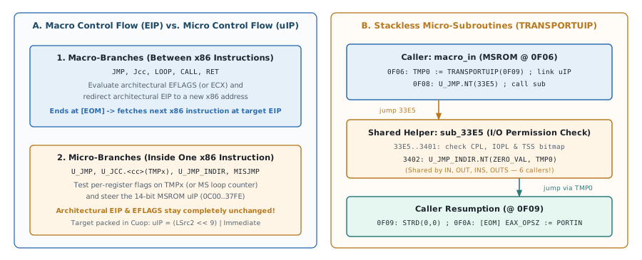
EIP between x86 instructions, whereas micro-branches steer the 14-bit µIP inside MSROM. Right: Stackless micro-subroutine linkage via TRANSPORTUIP and U_JMP_INDIR.3.1 Macro-Branches: Moving Architectural EIP
Ordinary x86 control-transfer instructions work much like they did on the 386 and 486:
- Conditional and unconditional relative jumps (
Jcc rel,JMP rel): Decode into a single[BOM.EOM]branchµop. InJNZ .loop, the Jump Execution Unit checksEFLAGS.ZF; ifZF == 0(the previous result was non-zero), it sets nextEIPtoEIP + relinstead of falling through toEIP + len. - Near
CALLandRET: Combine stack memoryµops with anEIPtransfer:CALL rel32pushes the returnEIPonto the stack (STRD+STAto[ESP - 4], plusESP := ESP - 4) and redirects fetch toEIP + rel32.RETpops the return address from[ESP]intoTMP0(LOAD), incrementsESPby4(ADD), and jumps toTMP0via[EOM] M_RET.- Even better, look at
RET imm16(pop return IP and releaseimm16bytes of stack arguments) orCALL regin theMSROMdisassembly:D0'sXLAT4emits the stack memory/pointerµops on cycle 1, then seamlessly continues into a one-line[EOM]MSROMtail (0F71: [EOM] M_RET(..., TMP0)forRET imm16, or1165: [EOM] M_CALL_INDIR(..., @REG_sss)forCALL reg) on cycle 2.
Here's a concrete example. This 12-byte real-mode snippet computes 5 + 3 + 2 + 1 = 11 (0x0B) in AX and halts—every instruction in the setup and loop body decodes into a single XLAT µop:
0000: B8 05 00    mov ax, 5        ; 1 XLAT uop:  AX := 5
0003: B9 03 00    mov cx, 3        ; 1 XLAT uop:  CX := 3
.loop:
0006: 01 C8       add ax, cx       ; 1 XLAT uop:  AX := AX + CX (FLAGS_ALL)
0008: 49          dec cx           ; 1 XLAT uop:  CX := CX - 1  (U2.1B: PF..OF, keep CF)
0009: 75 FB       jnz .loop        ; 1 XLAT uop:  if !ZF, EIP := 0006
000B: F4          hlt              ; MSROM @ 25EC
3.2 Micro-Branches Inside MSROM: Moving µIP in an Out-of-Order Core
The way control flow works at the µop level, however, is more subtle—and the reason comes straight down to out-of-order execution.
On an in-order microcoded CPU like the 386, the microsequencer and ALU step in lockstep: a micro-branch tests the ALU flags just produced and immediately picks the next ROM address. On P6, by contrast, the Microcode Sequencer (MS) sits in the in-order front end, pumping up to three Cuops per cycle into the Reservation Station many cycles before those µops actually execute.
How can MS branch on a TMP register whose value hasn't even been computed yet? As Intel's branch-handling patent (patent US5729728) explains, P6 treats micro-branches just like macro-branches—sending them into the Reservation Station and Jump Execution Unit (JEU) tagged with a 1-bit Mu (Macro/Micro) flag so they steer the 14-bit µIP while leaving architectural EIP untouched:
U_JMP.NT(target): Unconditional direct jump to a 14-bitMSROMaddress. Notice a clever bit-packing trick in the 72-bitCuop: because an unconditional jump has noLSrc2register to read, P6 concatenates(LSrc2<< 9) |Immediate(IA_UADDR) to encode a full microaddress without widening the 9-bitImmediatefield.U_JCC.<T|NT>.<cc>(TMPx, target): Conditional micro-branch testing a per-register flag (Z,NZ,C,NC, etc.) onTMPx. BecauseMScannot stall waiting forTMPxto execute out of order, everyU_JCCcarries a static prediction bit (.Ttaken or.NTnot-taken) in its opcode:MSimmediately keeps fetching along that predictedµIPpath, and ifJEUlater evaluatesTMPxand finds the static hint was wrong,JEUflushes the front end (JEClear) and restartsMSat the rightµIP.
3.3 Why P6 Has No Microcode Call Stack (TRANSPORTUIP)
Now consider microcode subroutines. Large MSROM flows share dozens of helper functions—checking I/O permission bitmaps, validating segment descriptors, or dispatching RDMSR/WRMSR addresses. On an in-order microcoded CPU (like the 386 or a classic VAX), you simply put a small 2- or 4-entry hardware return-address stack inside the microsequencer.
Why didn't P6 do that? Look at what happens to a hardware call stack inside MS once µops execute speculatively and out of order:
- Speculative pushes and pops:
MSfetches and issues microcode ahead of execution—potentially down a mispredicted macro-branch (Jcc) from theBTB, or past unresolvedU_JCChints insideMSROMitself. Worse, inJEU, a younger branch can even execute before an older branch (patentUS5729728Figs. 7b–7c), or a memoryµophalfway through a subroutine can page-fault (#PF) at retirement. IfMSpushed and popped a dedicated hardware stack at issue time, every branch misprediction or fault flush would leave that stack out of sync unless P6 built full checkpoint-and-rollback hardware for it. - Why macro
CALL/RETin 3.1 was easy by comparison: Architectural x86CALLandRETdon't keep their authoritative state in a hidden front-end stack either—they emit ordinaryµops that write the returnEIPinto[ESP](buffered safely in theMOBstore buffer with renamedESP) andLOADit back intoTMP0. (TheBTB's Return Stack Buffer is purely a speculative hint verified byJEU.) Microcode, of course, cannot push internalµIPs onto the user program's[ESP]stack.
Instead, P6 uses the exact same link-register idea as RISC architectures (jal ra, target / jr ra), storing return µIPs in ordinary TMP registers (right half of the diagram above; see the TRANSPORTUIP entry on Martin Hinner's P6 wiki):
TMPx :=TRANSPORTUIP(return_uip): Materializes a 14-bit literalMSROMreturn address into any general temporary register (TMP0,TMP8,TMPE, ...), immediately followed byU_JMPto the helper.U_JMP_INDIR.NT(ZERO_VAL, TMPx): At the end of the shared helper, an indirect micro-jump reads the returnµIPout ofTMPxinJEUand redirectsMSback to the caller.
By turning a return address into ordinary TMP register data, P6 gets out-of-order subroutine tracking and rollback for free from its existing register renamer (RAT + ROB): each TRANSPORTUIP allocates a fresh ROB entry, U_JMP_INDIR waits in the Reservation Station until that ROB entry is ready, and any branch misprediction or fault flush automatically discards speculative TMP writes with zero extra sequencer state.
Look at IN EAX, DX (macro_in at 0F06 in the MSROM disassembly, ending with PORTIN at 0F0A) calling the shared I/O permission helper sub_33E5 (33E5)—a single helper shared by six different callers (IN, OUT, INS, OUTS, and their REP variants):
; D0 XLAT4 prefix prepares port (TMP1 := zero_ext(DX)) and byte width (TMP2 := 1/2/4)
; Then MSROM continues at 0F06:
macro_in:
0F06: TMP0 := TRANSPORTUIP(0F09)                ; Save return microaddress 0F09 into TMP0
0F08: U_JMP.NT(33E5)                            ; Jump to shared I/O permission helper sub_33E5
...
sub_33E5:                                       ; Shared by 0F08, 1850, 18C8, 21DC, 261C, 2631
33E5: TMP3 := MOVE.DSZ32(ZERO_VAL)
33E6: TMP7 := MOVE.DSZ32(#1)
33E8: TMP4 := PSELECT_IO_BITMAP(TMP3, TMP7)     ; Hardware mode predicate: real mode / CPL<=IOPL vs VM86/bitmap
33E9: U_JCC.T.NZ(TMP4, 33FA, IA_UADDR)          ; Static .T hint: allowed -> skip TSS bitmap walk
...                                             ; [33EA..33F9: walk TSS I/O permission bitmap; #GP if denied]
@sub_33E5_permission_return:
...                                             ; [33FA..3401: finalize macro IP / helper cleanup]
3402: U_JMP_INDIR.NT(ZERO_VAL, TMP0)            ; Return to caller (0F09)
...
@macro_in_permission_return:
0F09: STRD.DSZ32(#0, #0)                        ; Dummy store-data companion paired with PORTIN in the MOB
0F0A: [EOM] EAX_OPSZ := PORTIN.ASZ16.SC1.@DSZ?(ZERO_OFFSET, TMP1, SEG.1)
Need a nested subroutine call inside another subroutine? An outer routine simply saves its return µIP in TMPE while the inner call uses TMP8—renamed independently in the ROB with zero hardware stack-depth limits.
4. Generic Programming with Micro-Ops: Macro Aliasing
Look back at the microcode excerpts we just read (CMPXCHG at 2651 and IN at 0F0A), and notice the @-marked operands and opcode modifiers:
@REG_sssand@REG_dddinstead ofEBXorECXEAX_OPSZinstead ofAL,AX, orEAXSUB.@DSZ?(...)andPORTIN.ASZ16.SC1.@DSZ?(...)instead of fixedDSZ8,DSZ16, orDSZ32
If you have ever written a generic function in C++ (template <typename T>) or Rust (fn cmpxchg<T>(...)) so you don't have to copy-paste the same algorithm for u8, u16, and u32, you already understand what P6's microcode engineers built in silicon.
Count the combinatorial explosion of x86 encoding if every XLAT entry and MSROM routine had to hardcode concrete registers and widths. Take a single instruction family like LOCK INC [mem] and LOCK DEC [mem]:
- 2 operations (
INCvs.DEC) - 3 data widths (
BYTE8-bit,WORD16-bit,DWORD32-bit, toggled by opcode bitWand the66hprefix relative toCS.D) - 2 address widths (
16-bit[BX+SI]vs.32-bit[EBX+ESI*4], toggled by67hrelative toCS.D) - 4 SIB index scales (
×1, ×2, ×4, ×8) across 8 base registers and 8 index registers - 6 possible segment overrides (
ES:,CS:,SS:,DS:,FS:,GS:)
Multiplying those combinations produces tens of thousands of legal x86 encodings—yet the entire Pentium Pro MSROM holds only 12,288 Cuop slots (8,448 in the main factory ROM region 0C00–37FE) for the entire IA-32 + x87 architecture.
4.1 From the 386 to P6: Instantiating Cuop Templates with MAR (Patent US5559974)
Size-generic microcode wasn't new to Intel—as we saw in z386, the 80386 already parameterized its 37-bit microcode to share routines across operand sizes and encodings:
- Symbolic register endpoints (
SRCREG,DSTREG) resolved fromModR/M, plus size-sensitive names likeeAX_ALvs.EAXandeIPvs.EIPvs.IP, - Opcode-derived ALU and shift operations (
+-&|^,<<>>?), and - A runtime
op_sizelatch (8/16/32-bit) initialized by the decoder—which 386 microcode could even override mid-routine (BITS8/BITS16/BITS32) and restore (BITSDE)—while hardwired front-end logic implicitly computed effective addresses (EA) beforeRDever ran.
Why couldn't P6 keep doing it the 386 way? Once again, out-of-order execution changes the contract:
- Every
µopin flight must be self-contained: On the in-order 386, the datapath executed one micro-instruction at a time for a single active x86 instruction, so the ALU could simply consult a globalop_sizeregister. On P6, the Reservation Station holds up to 20µops from many different x86 instructions at once—mixing 8-, 16-, and 32-bit operations, differentModR/Mregisters, and different segments out of order. Execution units (IEU,AGU) cannot peek back at decoder latches or share a mutableBITS16/BITS32flip-flop; everyµopenteringRATmust already carry concrete registers and widths. - Unified
XLAT+MSROMtemplates with explicit addressing: On P6, fast-path decoders (XLAT) andMSROMemit the exact same 72-bitCuopformat, and there is no separate pre-executionEAbox hiding beforeRD—memoryµops (LOAD,STA,LEA) must explicitly name their resolved base/index registers, scale, displacement, and segment.
P6 solves both problems by moving all template specialization into a combinational expansion stage right after XLAT and MSROM. Every 72-bit Cuop is treated as a stateless generic template, instantiated on the fly by a decoder latch called the Macro-Alias Register (MAR) (detailed in Intel's alias-expansion patent, patent US5559974):
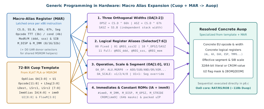
MAR) instantiates a 72-bit Cuop template across widths, logical registers, operations/segments, and immediates into a concrete Auop.When the Instruction Decoder parses an x86 instruction, a parallel Field Extractor latches the instruction's decoded parameters into MAR and holds them steady for the entire macroinstruction (from [BOM] to [EOM]):
- Active code/stack defaults (
CS.D,SS.B) and66h/67h/ segment-override prefixes, - The primary opcode's 3-bit ALU code (
TTT) or 4-bit condition code (tttn), ModR/M(mod,reg/ddd,rm/sss) andSIB(scale,index,base),- The extracted memory displacement (
M_DISP) and immediate (M_IMM).
As each 72-bit Cuop leaves XLAT or MSROM, combinational Alias Muxes substitute fields from MAR whenever the Cuop's alias control bits (OA, Selector[7:6], U1, IA) ask for them—producing a concrete Alias-resolved µop (Auop).
Let's tour the four things MAR can specialize on the fly.
4.2 Dimension 1: Three Orthogonal Widths (OPSZ, ASZ, and SASZ)
x86 actually has three independent width settings. Suppose a 32-bit protected-mode program (CS.D = 1) whose stack segment happens to be 16-bit (SS.B = 0) executes 66 67 FF 33 (PUSH WORD PTR [BX]):
OPSZ(Operand Size =CS.D ^ 66h= 16-bit): It reads and pushes 2 bytes of data.ASZ(Address Size =CS.D ^ 67h= 16-bit): It forms the source address from 16-bit[BX], not[EBX].SASZ(Stack Address Size =SS.B= 16-bit): It decrements and indexesSP, notESP—and noticeSASZignores both66hand67h.
Now remove 67h (66 FF 33, PUSH WORD PTR [EBX]): OPSZ is 16-bit, ASZ is 32-bit ([EBX]), and SASZ is still 16-bit (SP).
P6 keeps OPSZ, ASZ, and SASZ as three completely independent width wires in MAR (verified across all eight raw data-size codes on 0619h hardware). Setting the OpAlias data-size bit (OA[2] = 1, marked with @ directly on the size modifier such as .@DSZ? / .@DSZ16, or trailing .@DSZ) or address-size bit (OA[3] = 1, marked .@ASZ32 / .@ASZ16 or .@ASZ) lets each individual Cuop pick which of the three contexts (OPSZ, ASZ, or SASZ) governs its data width and address width while keeping the raw template bits visible.
4.3 Dimension 2: Logical Register Aliases (Selector[7:6])
Every Cuop has three 8-bit register fields: LDest, LSrc1, and LSrc2. Just looking at the top two bits (Selector[7:6]) tells the Alias Muxes how to resolve the register view (see also the wiki's registers table):
Bits [7:6] |
Selector Class | Examples in Disassembly | How MAR Resolves It |
|---|---|---|---|
00 |
Direct (Fixed) | EAX, AL, AX, TMP0..TMPE, CONST, SINK |
No alias—uses the exact register and width encoded in the Cuop. |
01 |
Identity Alias, Fixed Width | @REG_sss16, @REG_sss32, ST(i) |
Register number (0..7) comes from ModR/M, but width stays fixed (e.g., MOV CR0, EAX always uses 32-bit @REG_sss32 even in 16-bit real mode). |
10 |
Fixed Register, Size Alias | EAX_OPSZ, ECX_ASZ, ESP_SASZ |
Register identity is fixed (A, C, or SP), while width (8/16/32-bit) tracks byte-opcode / OPSZ, ASZ, or SASZ. |
11 |
Full Identity + Size Alias | @REG_ddd, @REG_sss, @REG_op, @REG_mem |
Both register identity and width come from MAR. @REG_ddd automatically becomes AL..BH on byte opcodes, AX..DI when OPSZ=16, and EAX..EDI when OPSZ=32. @REG_mem expands LSrc1 to the index register and LSrc2 to the base register across both 16-bit [BX+SI] and 32-bit [EBX+ESI*scale] modes. |
Look how much work ESP_SASZ and EAX_OPSZ save: PUSH templates simply address [ESP_SASZ] and subtract M_OPSZ from ESP_SASZ, automatically handling 16-bit SP stacks and 32-bit ESP stacks with zero branches.
4.4 Dimension 3: Operation, Scale, and Segment Aliases (OA[1:0] & U1)
P6 doesn't just alias registers and widths—it can alias the opcode itself:
OA_OP(OA[1]= 1,.@MGRP0/.@OP): WrittenALU.@MGRP0.@DSZin the disassembly (combiningOA[1]+OA[2], rawOA= 6), this replaces base opcodeMOVEwith the macroinstruction's decoded arithmetic operation (ADD,OR,ADC,SBB,AND,SUB,XOR,INC,DEC, orBTS/BTR/BTC). That meansADD r, [m],SUB r, [m],AND r, [m],OR r, [m], andXOR r, [m]across 8-, 16-, and 32-bit sizes all share one 2-CuopXLATtemplate (shown here fromp6.c's authoredXLATtable, matching AP-526's 2-µopcount):
; Authored XLAT Group 002 in p6.c — one 2-Cuop template for 8/16/32-bit ADD/SUB/AND/OR/XOR reg, [mem]
[BOM] TMP0     := LOAD.@ASZ32.@SC1.@DSZ?.0(@REG_mem, M_DISP, U1.1)
[EOM] @REG_ddd := ALU.@MGRP0.@DSZ(@REG_ddd, TMP0, FLAGS_ALL)
OA_SCALE(OA[0]= 1,.@SC1...@SC8/.@SC): Substitutes address scale factors—scaling offsets by operand byte count (×2or×4in measured@SC2/@SC8forms) and pairing with decoded SIB index addressing (×1, ×2, ×4, ×8) on memory/LEAtemplates (often combined withOA[3:2]as.@ASZ32.@SC1.@DSZ?or.@ASZ.@SC.@DSZ, rawOA= 0Dh).U1= 1(SEG_ALIAS): ReplacesLSegwith the instruction's effective segment—automatically selectingSSfor[EBP]/[ESP]base addressing,DSotherwise, orES/CS/SS/DS/FS/GSwhen a segment-override prefix is present.
4.5 Dimension 4: Immediates and the 64-Bit Constant ROM (CROM)
A 72-bit Cuop only has room for a 9-bit Immediate [12:4] field. How does a µop use a 32-bit x86 displacement, a 32-bit immediate, or the ASCII string "GenuineIntel"?
The 5-bit IA [17:13] (ImmAlias) field steers an immediate multiplexer:
- Inline 9-bit literal (
#n): A sign-extended small integer-256..+255encoded directly inside theCuop. Throughout our disassembly listings, a leading#denotes a literal constant value (#1=1,#8=8,#32=32), distinguishing it from register names or memory addresses. - Decoded x86 fields from
MAR:M_IMM(the decoded 8/16/32-bit immediate),M_DISP(the decoded 8/16/32-bit memory displacement),M_OPSZ(1,2, or4), orM_STRIDE(DF-signed ±1, ±2, ±4). - Companion Constant ROM (
CROM): When microcode needs a wide 32- or 64-bit constant,imm9indexes a 512-entry Constant ROM (CROM). Look atmacro_cpuid(2924–292C) in theMSROMdisassembly whenEAX == 0:
; MSROM disassembly: CPUID leaf 0 vendor string (MSROM @ 2924)
2924: TMPC := SUB.DSZ32(EAX, ZERO_VAL)          ; EAX == 0? (per-register ZF on TMPC; EFLAGS untouched)
2925: U_JCC.NT.NZ(TMPC, 292D, IA_UADDR)         ; Non-zero -> check leaf 1 / leaf 2
2926: EAX  := MOVE.DSZ32(#2)                    ; Inline 9-bit literal: max leaf = 2
2928: EBX  := MOVE.DSZ32(0x756E6547)            ; CROM_S2.12B -> "Genu"  (EBX:EDX:ECX = "GenuineIntel")
2929: ECX  := MOVE.DSZ32(0x6C65746E)            ; CROM_S2.0E3 -> "ntel"
292A: EDX  := MOVE.DSZ32(0x49656E69)            ; CROM_S2.170 -> "ineI"
292C: U_JMP.NT(375D)                            ; Jump to shared CPUID [EOM] exit
5. Putting It All Together: One 8-µop Routine, Hundreds of x86 Instructions
Let's watch every concept from this post—MSROM triads, [BOM]/[EOM] boundaries, split stores, two-tier U2 flags, micro-jumps, and MAR Macro Aliasing—work together in one routine. Here is macro_lock_inc_dec (12A5–12AC) and its shared 2-line store tail (2510–2511) from the Pentium Pro (CPUID 0619h) MSROM:
; MSROM disassembly: LOCK INC [mem] and LOCK DEC [mem] for all sizes, segments & addressing modes
macro_lock_inc_dec:
12A5: [BOM] MS_ENTRY(INST.014, INST.014)                             ; MSROM entry marker starting macroinstruction
12A6: STRD.DSZ32(ZERO_VAL, ZERO_VAL)                                 ; Dummy store-data companion for MOB_FENCE
12A8: MOB_FENCE(ZERO_OFFSET, ZERO_OFFSET)                            ; Drain prior stores before bus/cache lock
12A9: TMP0 := XLOAD.LOCK.@ASZ.@SC.@DSZ(@REG_mem, M_DISP, U1.1)       ; Locked load into TMP0
12AA: TMP0 := ALU.@MGRP0.@DSZ(TMP0, #1, U2.1B)                       ; INC or DEC by 1; update PF..OF, keep CF
12AC: U_JMP.NT(2510)                                                 ; Jump to shared LOCK store tail (note: 12AB doesn't exist)
...
helper_lock_rmw_store_tail:                                          ; Shared by 6 different LOCK instruction families
2510: STRD.DSZ32(ZERO_VAL, TMP0)
2511: [EOM] STA.LOCK.@ASZ.@SC.@DSZ(@REG_mem, M_DISP, U1.1)           ; Write back & release lock at [EOM]
Feed two completely different x86 byte sequences into those exact same eight Cuop words:
- 32-bit mode (
CS.D = 1):F0 FE 44 B3 10→lock inc byte ptr [ebx + esi*4 + 0x10]- At
12A9,.@ASZ.@SC.@DSZ+@REG_mem+U1.1+M_DISPexpands to an 8-bit locked load fromDS:[EBX + ESI*4 + 0x10]. - At
12AA,ALU.@MGRP0.@DSZbecomesADD.DSZ8(TMP0, 1), andU2.1BupdatesPF, AF, ZF, SF, OFfrom that 8-bit sum while leavingEFLAGS.CFuntouched. - After
12ACjumps to2510(skipping non-existent triad slot12AB),STRD+[EOM] STA.LOCK.@ASZ.@SC.@DSZwrites the updated byte back toDS:[EBX + ESI*4 + 0x10].
- At
- 16-bit mode (
CS.D = 0) withES:and66hprefixes:26 66 F0 FF 0F→lock dec dword ptr es:[bx]- Without changing a single bit in
MSROM,12A9now expands to a 32-bit locked load (CS.D ^ 66h = 1) using a 16-bit[BX + 0]effective address (CS.D ^ 67h = 0) in segmentES:(U1.1). 12AAbecomesSUB.DSZ32(TMP0, 1), again preservingCFviaU2.1B, and2511writes all 4 bytes back toES:[BX].
- Without changing a single bit in
Wrapping Up
Stepping back, we can see why P6's front end was such a clean break from the 386, 486, and original Pentium:
- Uniform internal operations: Variable-length x86 instructions crack into fixed-format
µops via fast 4-1-1XLATdecoders (1–4 µops) or 3-slotMSROMtriads, bracketed by[BOM]and[EOM]. - Two-tier flags (patents
US5574942&US6047369): Storing per-register flags alongside every register's value lets microcode compute, branch (U_JCC), and conditionally move (MERGE/CMOV) without touching architecturalEFLAGS, whileU2masks publish exact x86 flag subsets (INC/DECvs.ADD/SUB) on demand. - Clean control-flow separation: Macro-branches move
EIPbetween x86 instructions, whileU_JMP,U_JCC, and register-linkedTRANSPORTUIP/U_JMP_INDIRsubroutines navigateMSROMwithout a hardware microcode return stack. - Macro Aliasing (
MAR): Parameterizing registers (@REG_ddd,@REG_mem,ESP_SASZ), orthogonal widths (OPSZ,ASZ,SASZ), operations (ALU.@MGRP0.@DSZ), segments (U1), andCROMconstants lets compactCuoptemplates cover the entire IA-32 encoding matrix.
This long post only covers the basics of P6's µop layer—we haven't yet touched deeper topics like protected-mode segmentation, paging, events, or the out-of-order backend itself. All of that front-end complexity paid off handsomely in performance. Where an i486 averaged roughly 0.5 instructions per clock on typical integer code (~2 CPI) and the dual-pipe in-order Pentium stalled whenever instructions failed to pair or missed in L1, P6's 3-wide out-of-order engine delivered roughly 40% more integer work per clock than Pentium (~1.5 vs. ~1.1 SPECint92/MHz). Even better, decoupling x86 decode into a deeper 14-stage µop pipeline scaled remarkably well in clock frequency: fabricated on the exact same 0.6 µm BiCMOS process where Pentium (P54C) topped out at 100 MHz, the first production Pentium Pro shipped at 150 MHz (6.08 SPECint95, nearly double a Pentium-100) and immediately reached 200 MHz on 0.35 µm. Over the next decade, direct P6 cores scaled past 1.4 GHz in Pentium III (Tualatin) and 2.26 GHz in Pentium M (Dothan).
Special thanks to Rudolf Marek (ruik) and Martin Hinner for reviewing this post, sharing their P6 microcode tools and research, and inspiring the inline @-modifier syntax used in the listings above.
References
- Robert P. Colwell, Dave B. Papworth, Glenn J. Hinton, Mike A. Fetterman, and Andy F. Glew, “Intel's P6 Microarchitecture,” Chapter 7 in John Paul Shen and Mikko H. Lipasti, Modern Processor Design: Fundamentals of Superscalar Processors, McGraw-Hill, 2005, pp. 329–367. Primary architectural overview of the P6 pipeline, 4-1-1 instruction decoders, register renaming, Reservation Station, and Reorder Buffer written by the P6 design team.
- David B. Papworth, “Tuning the Pentium Pro Microarchitecture”, IEEE Micro, August 1996, pp. 8–15. Documents the 14-stage pipeline, 4-1-1 decoder trade-offs, and 150 MHz 0.6 µm / 200 MHz 0.35 µm silicon results.
- Intel Corporation, Optimizations for Intel's 32-Bit Processors, Application Note AP-526 (Order No. 242816-001), October 1995. Appendix D provides Intel's published
µopcounts and execution-port breakdowns for shortXLAT-decoded P6 instructions. - Darrell D. Boggs, Gary L. Brown, Michael M. Hancock, and Donald D. Parker, “Decoder Having Independently Loaded Micro-Alias and Macro-Alias Registers Accessible Simultaneously by One Micro-Operation”, U.S. Patent 5,559,974, 1996. Defines
Cuoptemplates, the Macro-Alias Register (MAR), Micro-Alias Register (UAR), and combinational expansion intoAuops. - Adrian L. Carbine, Gary L. Brown, and Donald D. Parker, “Decoder for Decoding Multiple Instructions in Parallel”, U.S. Patent 5,630,083, 1997. Describes instruction-length decoding, byte steering, and P6's asymmetric 4-1-1 (
D0/D1/D2) parallel decoder arrangement. - Robert P. Colwell, David B. Papworth, Michael A. Fetterman, Andrew F. Glew, Glenn J. Hinton, Stephen M. Coward, and Grace C. Chen, “Hybrid Execution Unit for Complex Microprocessor”, U.S. Patent 5,574,942, 1996. Details per-register integer and floating-point
Flagsfields carried alongside operand data, carry-in sourcing, and flag-data merge operations (WUMERGE.FLAGS). - Robert P. Colwell, Andrew F. Glew, Atiq A. Bajwa, Glenn J. Hinton, and Michael A. Fetterman, “Flag Renaming and Flag Masks Within Register Alias Table”, U.S. Patent 6,047,369, 2000 (filed 1994). Explains masked architectural
EFLAGSupdates, partial-flag renaming (INC/DECvs.ADD/SUB), and flag-mask decoding. - Robert P. Colwell, Atiq Bajwa, Michael A. Fetterman, Andrew F. Glew, Glenn J. Hinton, and David B. Papworth, “Method and Apparatus for Predicting, Clearing and Redirecting Unpredicted Changes in Instruction Flow in a Microprocessor”, U.S. Patent 5,729,728, 1998. Covers macro- vs. micro-branch tagging (
Mu), static.T/.NTprediction in the microcode sequencer, and out-of-order branch verification and clearing inJEU. - Glenn J. Hinton, David B. Papworth, Andrew F. Glew, Michael A. Fetterman, and Robert P. Colwell, “Method for Pipeline Processing of Instructions by Controlling Access to a Reorder Buffer Using a Register File Outside the Reorder Buffer”, U.S. Patent 5,721,855, 1998; and Michael A. Fetterman, Andrew F. Glew, David B. Papworth, Glenn J. Hinton, and Robert P. Colwell, “Speculative and Committed Resource Files in an Out-of-Order Processor”, U.S. Patent 5,627,985, 1997. Overall P6 pipeline boundaries,
RATrenaming, andROB/RRFspeculative vs. committed data-and-flags storage. - Bradley D. Hoyt et al., “Method and Apparatus for Implementing a Set-Associative Branch Target Buffer”, U.S. Patent 5,574,871, 1996; and Andy Glew, Glenn Hinton, and Haitham Akkary, “Method and Apparatus for Performing Page Table Walks in a Microprocessor Capable of Processing Speculative Instructions”, U.S. Patent 5,680,565, 1997. Companion P6 front-end branch prediction and speculative paging patents cited in the introduction.
- Peter Bosch (
peterbjornx),p6toolsand “Under the Hood of a Pentium II”; Rudolf Marek (ruik),utools,patchtools_pub, andmicrocode-patch-collection; and Martin Hinner, P6 Microcode Wiki. Community reverse-engineering references for P6 microcode update keys, ROM dumping, triad scrambling, 72-bitCuopbit layouts,CRBUSaccess, andµopmnemonics.
Comments