Recreating Voodoo Graphics and a Late-1990s Gaming PC on an FPGA
I've spent the last month adding features and improving performance in z486_MiSTer, mostly working through games from the first half of the 1990s. Looking a few years ahead brought me to another change I wanted to explore: the arrival of 3D graphics cards.
The first one that left a strong impression on me was the Voodoo. The game was Need for Speed II SE. Smooth textures, fog, and the speed of the whole thing made it feel like a new generation of PC gaming. Could I recreate that on an FPGA now that the z486 CPU exists?
The result of this detour is zSST, a SystemVerilog implementation of the 3dfx Voodoo Graphics, or SST-1. Combined with my z486 CPU and the surrounding PC hardware, it forms z486 XL: a DOS PC with Voodoo graphics running in the programmable logic of a Xilinx KV260 board. Tomb Raider now runs with its original 3dfx renderer.
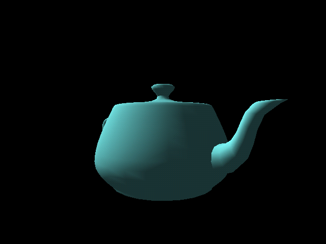
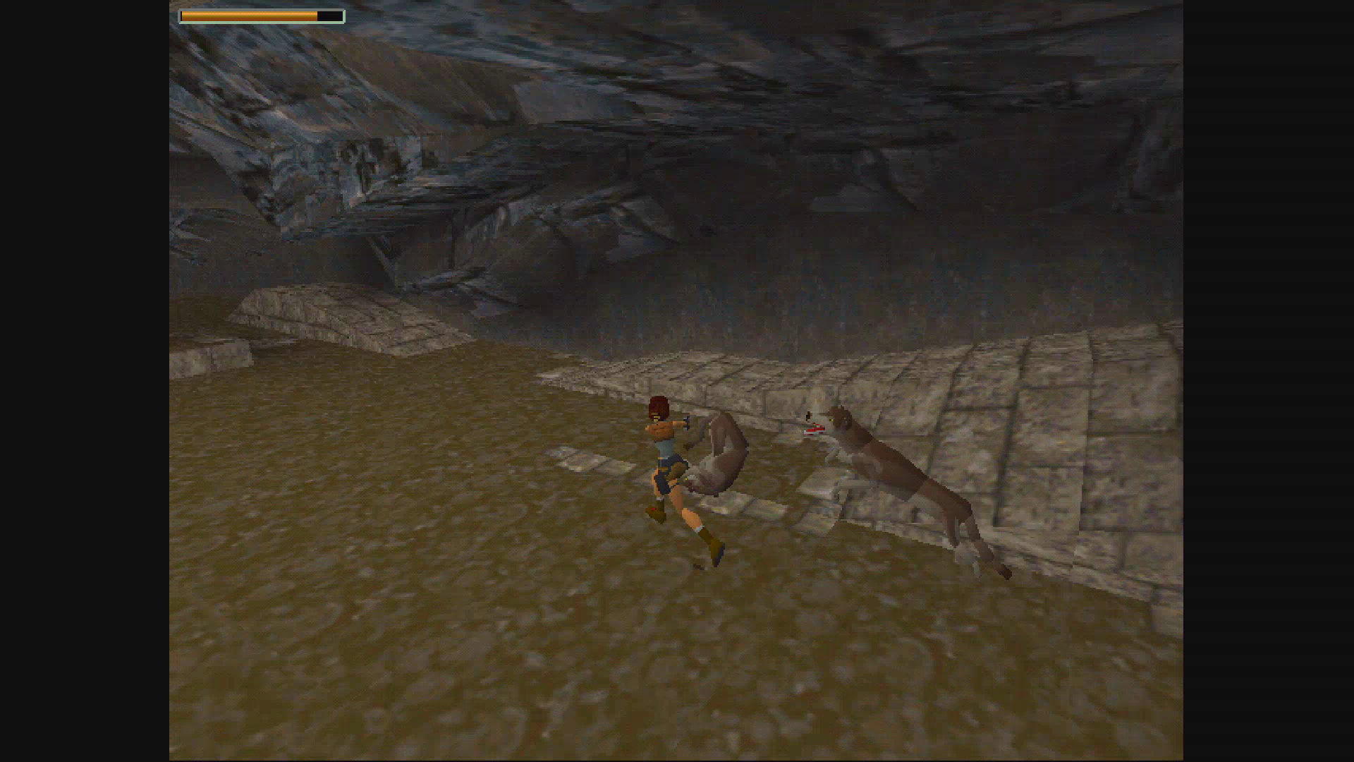
zSST implements most of the central Voodoo features: prepared triangles, texture filtering and mipmapping, depth and alpha tests, fog, blending, dithering, framebuffer access, and buffer swaps. It supports both the fixed-point and floating-point setup interfaces. Hardware game testing is still concentrated on Tomb Raider; broader compatibility and later Voodoo generations are work for another day.
The CPU and renderer run at 100 MHz on the KV260. That board has enough logic, DSP blocks, on-chip memory, and DDR bandwidth for the combined design. The DE10-Nano does not have room for this graphics addition. The KV260 uses its onboard DDR; there is no external SDRAM module to add.
Starting from the programming model
Fortunately, there is plenty of material to work from. 3dfx released the Glide source in 1999, before NVIDIA acquired its core graphics assets in December 2000. The surviving Glide source and SST-1 specification explain how software prepares triangles, configures the pixel pipeline, and manages textures and framebuffers.
The specification is a behavioral target, rather than a circuit diagram. It tells what should happen when software writes a register, but leaves many implementation choices open. 86Box provides useful references for complicated rendering behavior. The earlier MAME Voodoo work is another part of this preservation history. SpinalVoodoo supplied particularly useful Glide traces and reference screenshots for testing.
From triangles to 3D, one pixel per clock
Voodoo Graphics turns triangles into pixels, leaving much of the 3D work to the host CPU. Its command interface is surprisingly compact: five main command registers drive the accelerator.
| Register | Action |
|---|---|
triangleCMD |
Start rendering a prepared triangle. |
ftriangleCMD |
Start a triangle through the floating-point setup interface. |
nopCMD |
Flush the pipeline; optionally reset the statistics counters. |
fastfillCMD |
Clear a clipped rectangle of color and/or depth data. |
swapbufferCMD |
Switch the displayed buffer, immediately or synchronized to vertical retrace. |
Both triangle commands launch the same rendering pipeline. Other registers hold coordinates, gradients, and render state, while memory-mapped regions provide texture uploads and direct framebuffer access. The main drawing primitive is simply a prepared triangle.
For game developers, Glide presents a friendlier interface:
void grDrawTriangle(const GrVertex *a, const GrVertex *b, const GrVertex *c);
Before this call, the host CPU transforms the 3D geometry, computes vertex lighting, clips it, and projects it onto the screen. Glide then prepares the screen-space triangle and its parameter gradients—the increments used to interpolate values across its surface—and writes the triangle command to start rendering. Unlike later GPUs such as the GeForce 256, SST-1 has no hardware transform-and-lighting engine.
That still leaves plenty of work for the accelerator. The rasterizer finds which pixel centers lie inside the triangle and interpolates their color, depth, and texture coordinates. The texture unit fetches and filters texels; the framebuffer unit combines colors, applies visibility tests and fog, blends with the existing image, and writes the result.
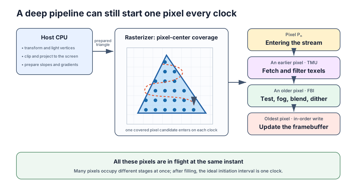
The original card divides this work between two ASICs: the FBI, or Frame Buffer Interface, and TREX, the texture mapping unit, usually called the TMU. At a 50 MHz graphics clock, the advertised peak is one textured, depth-tested output pixel per clock: 50 million pixels per second.
One pixel per clock does not mean that a pixel finishes in one clock. It means that different stages can work on different pixels simultaneously: while one pixel is being textured, an earlier one can be blended and another written out. Once the pipeline is full, it can ideally accept and finish a pixel every clock, provided memory keeps up.
That is the appeal of a fixed-function pipeline. A software renderer executes many instructions for each pixel; dedicated hardware overlaps that work across a steady stream of pixels. Voodoo brought richly textured 3D games to life at a fluid 30 FPS or more—a big part of what made it so popular.
Building the pixel pipeline
Compared with an x86 CPU, the arithmetic path is pleasantly regular. Let's follow a pixel from its interpolated parameters through texturing and color operations to the framebuffer, starting with how the numbers are represented.
Fixed point behind a floating-point interface
Floating-point arithmetic is central to modern GPU programming. SST-1 sits at an interesting transition: software can submit floating-point values, but the rendering machinery largely operates in fixed point—integers with an implicit scale factor.
| Setup value | Fixed-point register format |
|---|---|
| Screen X and Y | 12.4 |
| Red, green, blue, alpha | 12.12 |
| Depth Z | 20.12 |
| Texture S/W and T/W | 14.18 |
| Reciprocal W | 2.30 |
Here 12.4 means twelve bits before the binary point, including the sign,
and four fractional bits. A screen coordinate of 10.5 is therefore stored as
the integer 168: multiply by 16 to encode it, divide by 16 to recover the
value. Those fractional bits let the rasterizer handle vertices between pixel
centers.
The fvertex, fstart, and floating-point gradient registers accept IEEE
single-precision values. SST-1 converts them into its internal fixed-point
representation, and zSST follows that contract. Once the triangle is prepared,
advancing along a scanline mostly means adding a precomputed increment to each
interpolated parameter. Much of the pixel-by-pixel work becomes simple integer
addition.
Four texels for one pixel
For perspective-correct texturing, the TMU interpolates S/W, T/W, and 1/W, then divides the first two by the third to recover texture coordinates. This keeps a floor or wall texture in perspective as the surface recedes. The TMU also selects a mip level: a smaller version of the texture for pixels that cover a larger area of its surface. This reduces aliasing and shimmering in the distance.
Bilinear filtering then combines four neighboring texels—the pixels of the texture—around the sample position. First blend the top pair horizontally, then the bottom pair, and finally blend vertically between those two results. The fractional position determines the weights, producing a smooth transition between texel colors instead of an abrupt jump from one to the next.
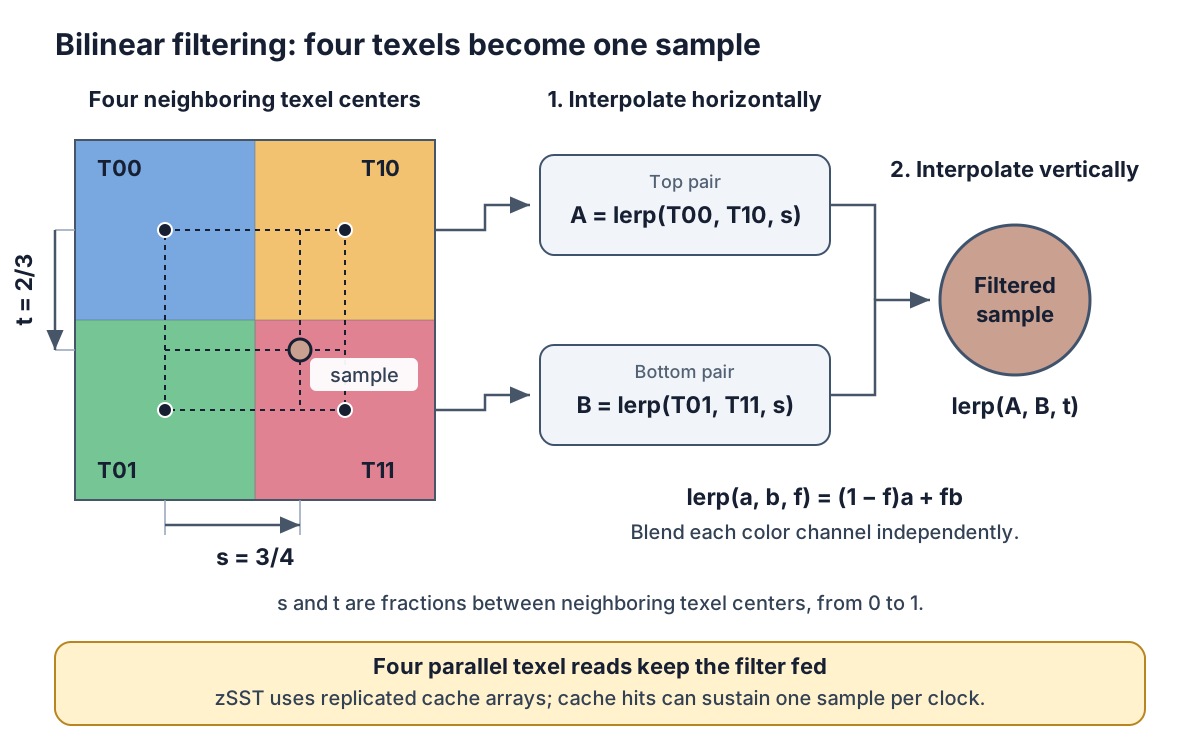
In zSST, a four-stage front end pipelines the perspective and level-of-detail calculations. Address generation and cache lookup supply the texels, and two registered decode stages turn their stored formats into colors for filtering and texture combining. Palette-based and NCC-encoded textures need different decoding rules, but ultimately feed the same pixel stream.
Color, tests, fog, and blending
Once texture and framebuffer data are available, zSST's FBI pixel path uses six registered stages:
| Stage | Main work |
|---|---|
| F0 | Select sources, check chroma key, prepare Z/W depth values. |
| F1 | Apply the color and alpha combine functions. |
| F2a | Test alpha/depth and look up the fog factor. |
| F2b | Apply fog. |
| F3 | Reconstruct destination color and perform alpha blending. |
| F4 | Convert to framebuffer precision, dither, and apply write masks. |
These stage boundaries are chosen to meet the FPGA's clock target. The SST-1 specification describes the operations but does not reveal the original ASIC's exact pipeline registers. Splitting fog lookup from fog application, for example, keeps a long arithmetic path out of a single clock while retaining the ability to accept one pixel per clock.
The result is written to the back buffer. A retrace-synchronized buffer swap then displays the finished image without switching buffers halfway through scanout. The original Voodoo was a 3D-only add-on, passing the ordinary VGA card's output through when inactive. z486 XL makes the analogous selection between the PC's VGA output and zSST's display output inside the FPGA system.
The hard part: feeding it from memory
The zSST pixel pipeline proved relatively straightforward to implement, at least compared with z486's CPU pipelines. Keeping it fed turned out to be much harder. A bilinear sample needs four texels from separate addresses. A depth-tested, blended pixel also needs the existing depth and color, followed by writes of the new values. Performing those accesses one at a time quickly destroys throughput. I ended up spending more time designing, tuning, and debugging the memory system than the arithmetic pipeline.
How the original card supplied the pixels
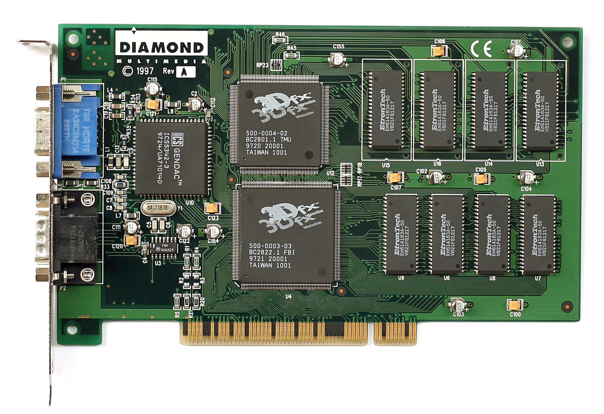
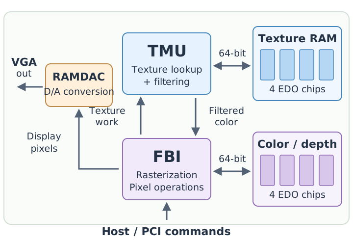
Photo: Konstantin Lanzet; crop: Pittigrilli, Wikimedia Commons. Photo license: GFDL 1.2 or later. Schematic: nand2mario.

The division of labor is visible on this Diamond Monster 3D. The upper 3dfx chip is the TMU, the lower one the FBI, each with four EDO RAM chips to its right. The upper group holds textures; the lower group holds color and depth/alpha buffers.
FBI and TMU each have a dedicated 64-bit memory path. On the texture side, four-way interleaving lets the banks read independent addresses, supplying the four neighbors for bilinear filtering in parallel. The specification (p. 13) promises the same throughput as point sampling, without storing duplicate texels.
But what if two neighboring texels land in the same chip? The trick is to distribute texels in a repeating two-dimensional pattern, rather than split the image into four large regions. Assign a bank to each combination of even or odd column and row, and the reason becomes clear:
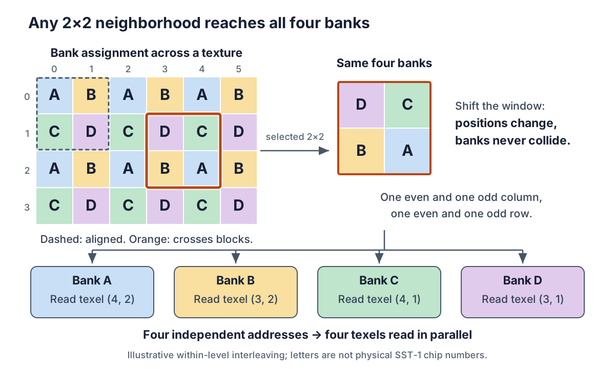
Every 2×2 window contains A, B, C, and D—even the orange window crossing both horizontal and vertical block boundaries. Two consecutive columns have opposite parity, as do two consecutive rows. All four combinations occur exactly once, so each bank supplies one texel with no conflict.
Texture edges and small mip levels need a little more care. SST-1 uses power-of-two texture dimensions, so wrapping preserves the alternating pattern for dimensions of two or more. At clamped edges, or in mip levels only one texel wide or high, some samples reuse the same texel. The central insight remains: fast bilinear filtering depends on arranging memory so that the arithmetic receives all its inputs together.
The FBI applies a similar idea to color and depth/alpha memory. Its interleaved path supports a peak of one rendered pixel per clock, or two pixels per clock for clears. Working on adjacent pixels together spreads the read/write cost across a scanline. Fabien Sanglard's two-pixel explanation offers a useful reconstruction of this behavior, though the exact ASIC bank schedule is not documented in the programming guide.
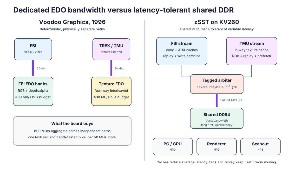
At 50 MHz, each 64-bit path has a theoretical bandwidth of 400 MB/s: 800 MB/s in total, but reserved for different jobs. The TMU cannot borrow idle FBI bandwidth, or vice versa. These dedicated buses and carefully arranged banks remind me of the NES- and SNES-era designs I explored in projects such as SNESTang: getting the most out of memory means designing around exactly when and where each value is needed.
What changes on an FPGA SoC
Voodoo's memory layout explains how it kept the pipeline busy, but I cannot simply transplant that design to the KV260. The board has much more memory bandwidth, yet no dedicated EDO memory attached to either rendering unit. Instead, the FPGA accesses shared DDR through the Zynq processing system's AXI ports. Linux, the FPGA PC, and display scanout all compete for that memory. The goal is the same—keep the pixel pipeline fed—but the way to achieve it has to change.
Our KV260 measurements show why bandwidth alone is not enough. A 128-bit port at 100 MHz has a theoretical bandwidth of 1.6 GB/s. With one request outstanding, a 4 KiB read reaches 1,370 MiB/s, but a 64-byte read reaches only 189 MiB/s. The first data typically takes about 280 ns to arrive—roughly 28 clocks at 100 MHz—with occasional much longer waits.
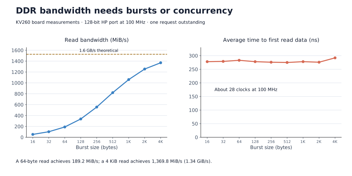
A renderer that waits for each small read before issuing the next will spend most of its time idle. zSST needs enough independent work in flight to cover those waits.
Caches, replay, and a reorder buffer
Keeping the pipeline fed requires both fewer DDR accesses and less time spent waiting for them. The first step is caching. Nearby screen pixels often sample overlapping parts of a texture, so recently fetched texels can be reused from on-chip RAM. zSST's texture cache holds 8 KiB in 64-byte lines; each fetch also brings in neighboring texels that subsequent pixels are likely to need.
A cache miss still takes many clocks, but independent texture samples need not wait for it. zSST keeps up to eight cache-line fetches outstanding, using a replay queue to park samples with missing data and retry them when it arrives. Meanwhile, samples whose texels are already cached can proceed. Prefetching gets a head start on future reads.
Now a later cache hit can finish before an earlier miss. A 64-entry reorder buffer, or ROB, collects those results and releases them in their original order. The principle is familiar from CPUs: do useful work during a long wait, then restore order before passing the results downstream.
The framebuffer side uses separate 4 KiB color and depth/alpha read caches, while write combiners pack neighboring 16-bit updates into 128-bit requests. Here, ordering matters: blending or depth testing may need a value that an earlier pixel has changed but not yet written to DDR. Forwarding supplies the pending value directly. Framebuffer updates take effect in order, and state changes that require completed work wait for it to drain. Memory requests can overlap, but later pixels must still see the effects of earlier ones.
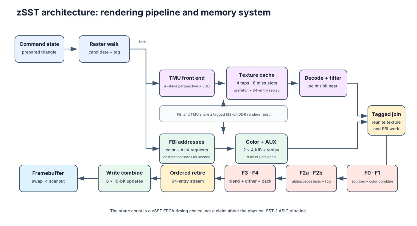
FBI and TMU share the renderer's 128-bit AXI port, HP2. The PC uses HP0 and display scanout uses HP3, keeping their request queues separate even though all three ultimately share DDR.
Evaluation results
I measure the renderer separately from the complete PC. The simulation benchmark sends commands through zSST's front end and exercises the TMU, FBI, shared arbiter, and a DDR timing model. Read data arrives after at least 26 clocks, with deterministic variation and occasional longer delays; writes are also rate-limited. The full-renderer tests allow 32 outstanding reads.
At 100 MHz, zSST reaches 78.5 million pixels per second (MPix/s) for textured triangles, and 72.8 MPix/s with depth testing and blending. Voodoo 1's published estimates at its native 50 MHz are 43 and 37 MPix/s for comparable feature sets. This is not an apples-to-apples benchmark: the triangle workloads differ, and the original estimates also include fog, mipmapping, and Gouraud shading. I do not have a Voodoo 1 to run the same test on both. The comparison shows the approximate fill-rate range, not a measured speedup over the original card.
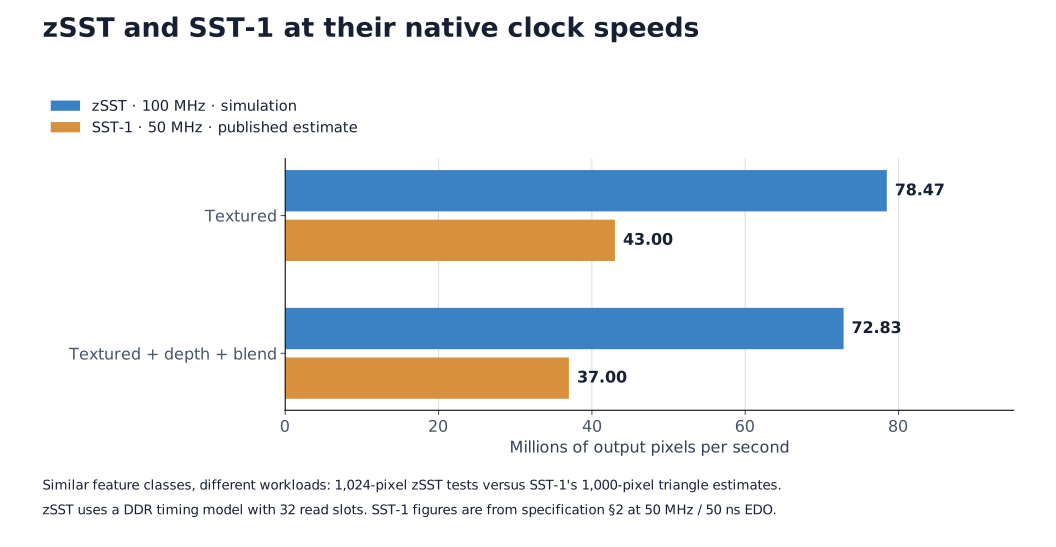
High fill rates do not automatically translate into high game FPS. On the board, Tomb Raider Level 2 produced 237 displayed buffer swaps in about 20 seconds—roughly 12 per second, measured from swaps rather than an engine FPS counter. Preliminary measurements point to a CPU bottleneck: it still has to run the game, prepare geometry, and submit commands. Shared DDR contention may also contribute. There is plenty left to optimize in the complete machine.
For non-Voodoo games, the current 100 MHz z486 XL runs maximum-detail Doom at 38.5 FPS and Quake 1.06 at 8.1 FPS. That is roughly 20% faster than the 85 MHz DE10-Nano build—about 23% for Doom and 19% for Quake. A 512 KiB write-back L2 cache in UltraRAM helps the CPU make better use of DDR.
In the integrated XCK26 build, zSST accounts for about 29,500 LUTs, 28,100 flip-flops, 14 RAMB36 blocks, 8 RAMB18 blocks, and 97 DSP slices. The combined PC and graphics design meets timing at 100 MHz.
Closing
The rewarding part is seeing original Glide software drive hardware I built in RTL. I expected the rendering arithmetic to be the hard part; getting data to it efficiently took more work. Voodoo's carefully interleaved EDO and zSST's caches and queues solve the same problem under very different constraints: a fast pixel pipeline is only useful when it has something to do.
Both zSST and z486 XL are available open source. If you already have a KV260, the z486 XL SD image provides the Linux support and application needed to launch your own DOS disk images.
Credits: Thanks to SpinalVoodoo for the Glide traces and reference screenshots, and to 86Box for its implementation references. Fabien Sanglard's The story of the 3dfx Voodoo1 is an excellent introduction to the original card's memory system.
Comments