z486: A 486-Class Pipelined FPGA CPU with Integrated Floating-Point
I released z386, an open-source 80386 CPU core, in May and added the 80386 early-start optimization in June. Early start overlaps address generation for one instruction with completion of its predecessor. It was an important 386 performance feature, but it also previewed the more systematic i486 pipeline. The MiSTer core needed more performance, so I continued in that direction and added further 486-class mechanisms.
The result is z486, an open-source, 80486-class pipelined x86 CPU written in SystemVerilog. It combines hardwired, pipelined execution for common instructions with microcode for complex architectural behavior.
z486 is not an i486 clone. Its design draws on three i486-inspired elements:
- a pipelined D1/D2 frontend;
- hardwired execution of common instructions, with microcode retained for complex instructions; and
- an experimental integrated x87 unit implementing the subset exercised by Quake.
On the same MiSTer system, the current core runs the Doom timedemo at 29.1 FPS at maximum detail, compared with 21.0 FPS on ao486. This is roughly 486DX2-66-class performance for the measured workload. Dhrystone reaches 0.330 DMIPS/MHz, versus 0.225 for z386 and 0.194 for ao486. These results show that a practical pipelined x86 CPU with broad architectural support, including x87, can fit on a mid-range FPGA.
The i486 five-stage pipeline
A finite-state or microcoded CPU limits combinational depth by performing decode, address generation, memory access, ALU work, and commit in separate cycles. This supports a high clock frequency but gives simple instructions a high cycles-per-instruction (CPI) count. Combining all work into one cycle reduces CPI but creates long paths through wide multiplexers and interconnect. Pipelining separates the work with registers and overlaps successive instructions.
Variable-length x86 instructions require a different stage division from the
classic RISC pipeline,
commonly written as IF-ID-EX-MEM-WB. The i486 uses five stages:
| Stage | Main work |
|---|---|
| FI | Fetch a 16-byte line into the instruction queue. |
| D1 | Decode prefixes, opcode, ModR/M structure, instruction length, and D2 actions. |
| D2 | Capture displacement or immediate data and calculate an effective address. |
| EX | Execute ALU or microcode work; access cache and TLB for memory instructions. |
| WB | Write an ALU or load result into the register file. |
The two decode stages replace the single RISC ID stage, and cache access occurs in EX rather than in a separate MEM stage. Microcoded instructions can use several EX cycles. One-clock throughput is therefore the common case, not a property of every instruction.
Intel's functional block diagram, reproduced with the references, shows how internal buses connect decode, address generation, translation, cache access, and execution.
Decoding variable-length x86 instructions
By the time the i486 was designed, x86 instructions already had a complex, variable-length encoding. Prefixes, two-byte opcodes, ModR/M and SIB bytes, displacements, and immediates are all optional, and some fields cannot be located until earlier fields have been interpreted. Earlier x86 frontends used sequential decode machinery that could take several clocks. The i486 instead divides decode into two explicit pipeline stages: D1 determines instruction structure and boundaries, while D2 captures literals and generates addresses.
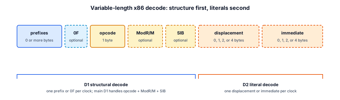
In the common case, D1 decodes the opcode, ModR/M, and SIB together. It also
determines the instruction length and tells the aligner where both the next
instruction and the current instruction's literals begin. Prefixes are
processed one byte per clock, and a 0F escape consumes another D1 clock.
D2 consumes one 1- to 4-byte displacement or immediate per clock. In parallel, it reads the base and index registers and calculates the effective address. Separate structural and literal ports in the prefetch queue let D1 work on one instruction while D2 works on its predecessor.
Common forms complete D2 in one clock. Two cases extend D2:
- an instruction with both a displacement and an immediate uses two D2 clocks;
- an address containing base, displacement, and scaled index can use a second D2 clock for the second addition.
This is also the pipelined version of the 386's early-start idea. On the 386, the instruction queue presents address operands during the final cycle of the previous instruction. On the i486, D2 is an explicit stage where the next instruction performs the same work while its predecessors occupy EX and WB.
The extra cycles are a deliberate area and timing tradeoff. Allowing both decoders to select every field from every possible byte position in the prefetch queue would require large alignment networks. The bounded D1 and D2 windows keep common instructions fast without making worst-case alignment part of the clock-critical datapath.
Loads, forwarding, and the pointer-load delay
Overlapping instructions introduce data hazards when a successor needs a result that its predecessor has not yet written to the register file. Consider a load followed immediately by an ALU operation:
mov eax, [esi]
add ebx, eax
When ADD reaches EX, the load result is in WB but may not yet be visible
through a normal register-file read. Stalling until the write completes would
create a data-load delay.
On the i486, given a cache hit, forwarding makes the value available to an ordinary dependent ALU instruction in the same cycle. Consequently, the i486 has no general data-load delay.
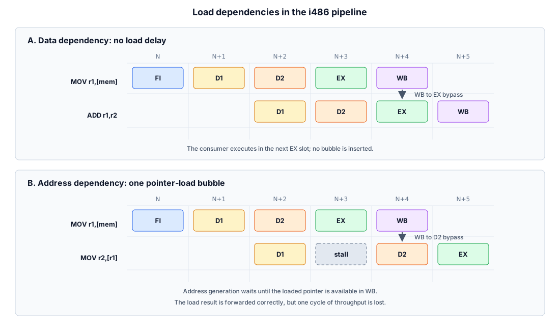
The exception is a successor that uses the loaded register as an address base or index:
mov eax, [esi]
mov ebx, [eax]
The second MOV needs EAX in D2 to calculate the effective address that its
memory access will use in EX. This is one stage earlier than an ALU consumer
needs the value. When the second instruction first reaches D2, the load is
still in EX and its result is unavailable. D2 must stall for one clock, then
receive the value when the load advances to WB. Intel called this the
pointer-load delay; today it is commonly described as an
address-generation interlock, or AGI.
Eliminating this delay would require an earlier and larger bypass network. The i486 instead accepts a one-cycle bubble for pointer dependencies.
Branch timing
The i486 evaluates a conditional branch in EX while speculatively fetching the target. A not-taken Jcc costs one clock because the sequential pipeline is already present. A taken Jcc, JMP, or near CALL takes three clocks from branch EX to target EX.
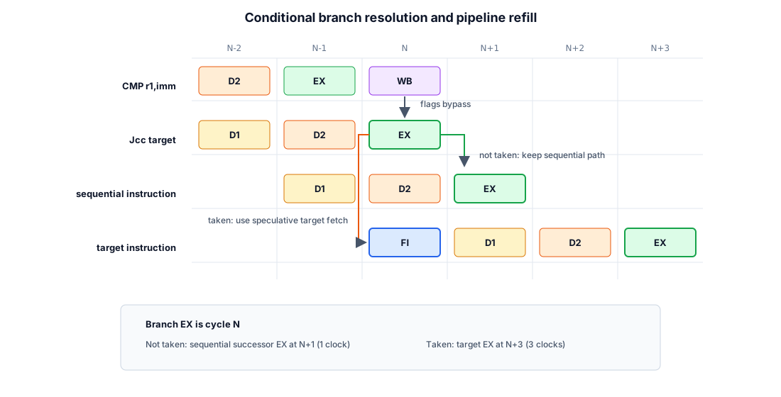
Crawford reports that Intel evaluated a more aggressive two-cycle taken-branch design, but it would have made not-taken branches slower and required significantly more cache machinery. The published instruction mix showed only about a one-percent overall advantage. The implemented three-cycle-taken, one-cycle-not-taken policy fit the rest of the pipeline better.
The z486 pipeline
Using the i486 pipeline as a guide, z486 retains its FI, D1, D2, and EX stage division. The main difference is at the back end: ordinary integer results commit on the EX edge rather than passing through a general WB stage.
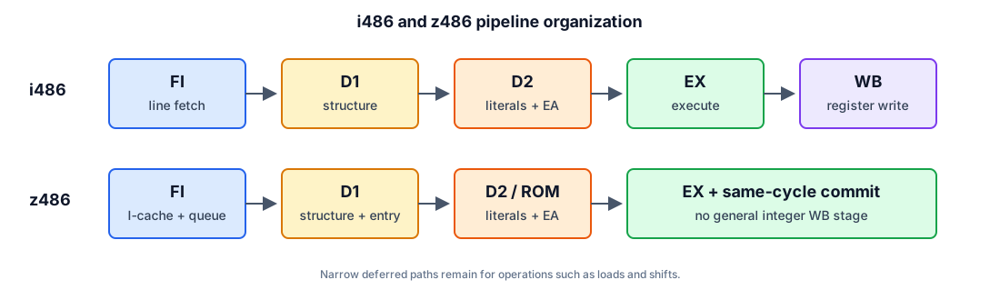
The implementation maps this stage flow onto hardwired and microcoded control
paths that share the same address, data, memory, protection, and floating-point
units. The RTL is also more modular than z386. Address generation, integer
execution, memory, hardwired control, and microsequencing were extracted into
separate modules, leaving z486.sv primarily as pipeline integration and
cross-unit glue. The resulting top-level module is about one-third shorter than
z386's: 2.6K lines versus 3.9K.
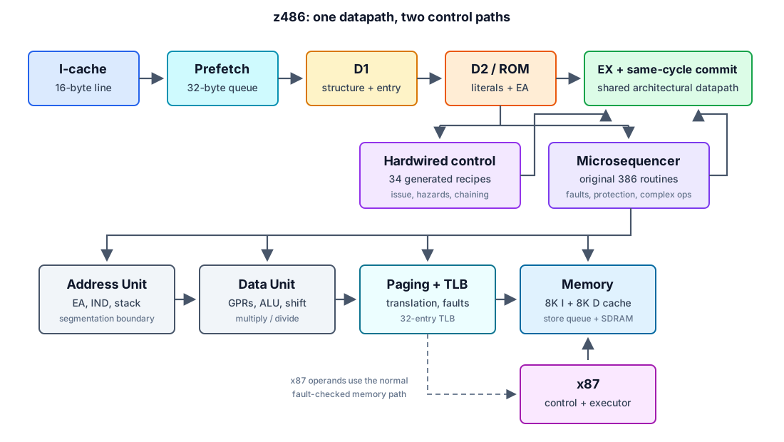
The frontend uses a 32-byte prefetch queue filled one 16-byte instruction-cache
line at a time. Like the i486 queue, it provides separate ports for structural
and literal decode: a registered 64-bit D1 window and a 32-bit literal window.
Prefixes and 0F consume extra structural cycles. An opcode and optional
ModR/M normally complete in one D1 clock, while SIB parsing can use a retained
sub-cycle. A one-entry registered skid buffer lets D1 run ahead when D2 is
occupied without requiring a deep decoded-instruction queue.
D1 resolves the microcode entry and launches it into the synchronous control
store. The first control word is therefore available in D2 alongside the
decoded instruction and its literals. D2 performs effective-address work and
hazard checks; i_issue is the single event that transfers the completed D2
instruction into EX.
This organization keeps two expensive operations out of the same cycle:
- D2 calculates and relocates the effective address to a linear address;
- the next part of the memory path translates it and accesses the physically indexed, physically tagged cache.
The release MiSTer configuration has separate 8 KB instruction and 8 KB data caches, both four-way set associative with 16-byte lines. The data cache is write-through with a three-entry store queue. The i486 instead has one unified 8 KB cache and completes a cache-hit load in one clock by overlapping virtual indexing with translation. z486 has twice the total L1 capacity, but its simpler physically indexed, physically tagged organization serializes translation and cache access. A best-case integer load therefore takes two clocks rather than the i486's one. Getting VIPT to work is future work.
Write-back organization
z486 differs from the i486 at the back end. Ordinary GPR, EIP, ESP, EFLAGS, and internal-register results commit on the EX clock edge; there is no general WB stage.
This is an FPGA-specific tradeoff. Preserving dependency timing with a full WB stage requires a broad bypass network: younger instructions need pending WB values in EX and, for address dependencies, one stage earlier in D2. In earlier experiments, the additional routing and operand-mux delay cost more than moving commit out of the EX critical paths saved. z486 therefore retains only narrow, operation-specific deferred state, such as a shifter result or a pending load commit.
Hardwiring common instructions
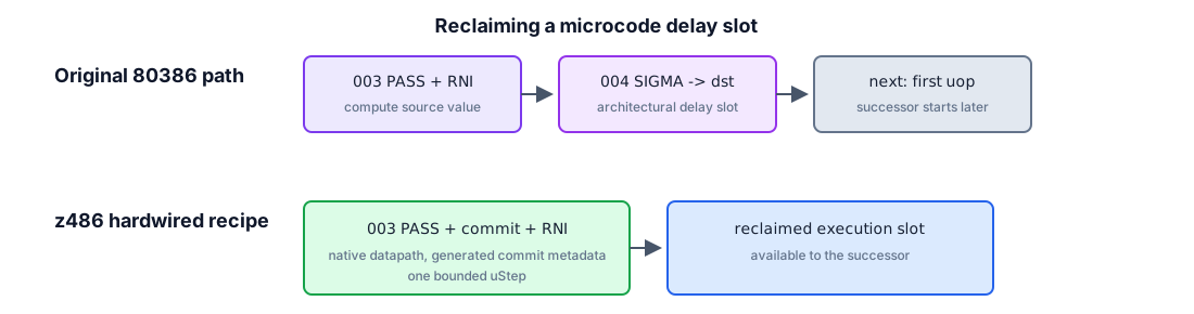
Pipelining does not automatically remove the original 386 microcode's
two-cycle minimum for simple operations. Register MOV, for example, is:
003  SRCREG                           PASS    RNI
004  SIGMA  -> DSTREG
The first word passes the source through the ALU and announces run-next-instruction (RNI). Because the sequencer has an architectural delay slot, the second word still executes and writes the result. Running this sequence unchanged would retain a two-cycle EX retirement rate despite the faster frontend.
The i486 controls frequent instructions with hardwired logic while retaining microcode for complex cases. z486 follows the same division: hardwired and microcoded control both drive the shared integer datapath.
Recipes and uSteps
The generation script scripts/ucode_optimize.py produces metadata for 34
hardwired instruction recipes. Each recipe contains one to three active
uSteps. A uStep combines a native microcode word with generated fields for
D2 work, architectural commit, delay-slot handling, and hazards.
For MOV r,r, the optimized word still uses the original PASS datapath, but a
generated destination encoding commits the ALU result on the same edge. The
hardwired recipe therefore completes the same work in one active slot.
Chaining
Once a delay slot is proven redundant, z486 may start the next hardwired instruction in it. This is called chaining. It applies to both one- and multi-uStep recipes: a one-uStep recipe can launch its registered successor at issue, while a multi-uStep recipe can launch the queue head when its final RNI word is approaching. Repeated one-uStep chains provide sustained one-instruction-per-clock execution.
Before chaining, the control unit checks:
- source, destination, and byte-register overlap;
- flags producer/consumer dependencies;
- effective-address base, index, and ESP dependencies;
- pending load and shift destinations;
- D2 and control-store residency;
- whether a memory or stack slot still contains real work; and
- faults, interrupts, traps, single-step, and CPU throttling.
Memory, stack, and branches
Recipes are not limited to register operations:
MOV r,[m]prepares the address in D2 and uses a two-uStep load recipe, retaining a real result slot;- stores and PUSH keep their memory slot because acceptance and ESP update are architectural work;
- safe not-taken Jcc can fold into the predecessor boundary;
- taken Jcc and JMP use the D2-computed relative target in one bounded branch uStep; and
- near CALL combines redirect, posted return-address store, and ESP commit.
The current best-case instruction timing is:
| Instruction class | 80386 | i486 | z486 |
|---|---|---|---|
MOV r,r / ADD r,r |
2 | 1 | 1 |
MOV r,[m] |
4 | 1 | 2 |
MOV [m],r |
2 | 1 | 1 |
ADD r,[m] |
5 | 2 | 3 |
| Jcc not taken | 3 | 1 | 1 |
| Jcc taken | about 9 | 3 | 3 |
| JMP taken | about 9 | 3 | 3 |
| near CALL | about 9 | 3 | 4 |
XCHG [m],r |
5 | 5 | 5 |
The main remaining gap is memory latency: z486's PIPT data cache takes two clocks for a load hit. A timing-safe VIPT design is one possible route to the i486's one-clock load.
Instructions without a hardwired recipe continue through the general microsequencer. Task switching, call gates, privilege transitions, descriptor updates, nested faults, unusual prefixes, and other complex behavior therefore retain the original microcode routines and their delay-slot assumptions.
Integrated x87 floating-point unit
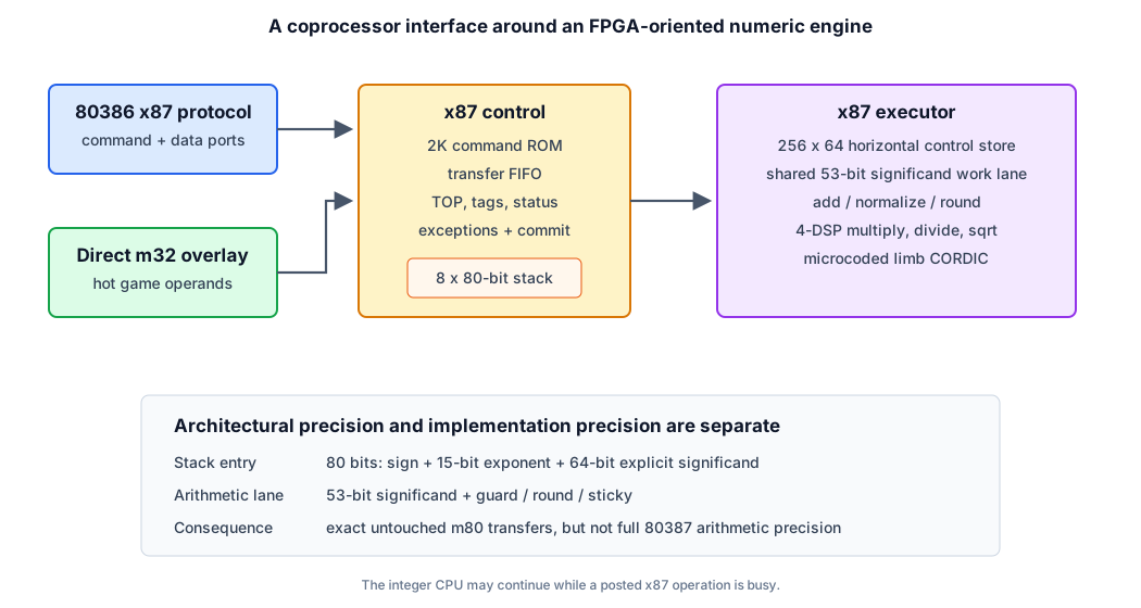
z486 includes an experimental integrated x87 floating-point unit. It is not yet a complete x87 implementation, but it implements enough of the instruction set to run Quake and TurboQuake. Its organization follows the major boundaries of the original 80387, whose block diagram appears in the references: command and stack control, a microcoded numeric executor, shared significand arithmetic, and a separate CORDIC engine for transcendental functions.
x87_bridgeconverts the 80386 command/data-port protocol into registered ready/valid transfers;x87_controlowns command decode, the stack, TOP, tags, status, exceptions, and architectural commit;x87_executorruns a generated 256-word horizontal control store over shared conversion and arithmetic resources; and- a qualified direct-m32 overlay removes the long 386 command/data transfer loop from common game instructions while preserving normal paging and fault checks.
The integer-only z386 core already occupied about 15,000 ALMs, while a complete PC configuration with caches, memory control, and peripherals exceeded 25,000. The Cyclone V on the DE10-Nano provides 41,910 ALMs, so a conventional FPU could easily exhaust the remaining capacity or make the design impractical to place and route. Three implementation choices keep the unit within this limited area budget:
-
Horizontal microcode and shared arithmetic. A synchronous 256-word by 64-bit control store sequences the numeric executor. Each horizontal word independently controls flow, operand preparation, classification, the add/subtract and shift routes, iterative engines, rounding state, result packing, commit, and CORDIC scratch accesses. This replaces a large decoded operation selector with direct control of the state updated by each step. Addition, normalization, conversion, and rounding share a 68-bit work register and adder. Division and square root reuse iterative datapaths, while the infrequent transcendental instructions use a microcoded, limb-oriented CORDIC engine.
-
Reduced internal precision. The architectural stack and transfer paths retain raw 80-bit temporary-real values, preserving untouched
FLD m80toFSTP m80round trips and save/restore data. Arithmetic decodes an operand into a 15-bit exponent and a 53-bit significand, with separate guard, round, and sticky state. The add/subtract path carries those 53 retained bits plus overflow and rounding positions in a 57-bit active slice of the shared work register. This keeps the 80387 exponent range but provides binary64-class precision rather than the 80387's full 64-bit significand. Results produced by arithmetic therefore have reduced precision even when stored as m80. -
DSP-based multiplication. The two 53-bit significands are split into 27- and 26-bit limbs. Four 27-by-27 products map onto Cyclone V DSP blocks and are assembled into an exact 106-bit intermediate product. This avoids a large LUT multiplier while retaining all bits needed by the common rounder.
With these measures, the FPU hierarchy uses about 5,100 ALMs in the 85 MHz release fit. The complete z486 PC build, including the FPU and peripherals, uses 35,686 of the DE10-Nano's 41,910 ALMs.
Performance was optimized iteratively as well. In an early TurboQuake render-window profile, x87 instructions accounted for about 23% of retired instructions but 61% of instruction-attributed cycles. The numeric executor was active during only about 40% of those x87 cycles; command dispatch, operand transfer, stack access, launch, and retirement consumed the rest. Performance work therefore addressed both sides of the CPU/FPU boundary: faster conversion and arithmetic schedules, a direct m32 path for common memory operands, and shorter command sequencing.
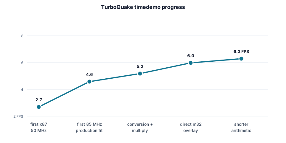
The first complete x87 build ran TurboQuake at 2.7 FPS at 50 MHz. The current release reaches about 6.3 FPS at the 85 MHz board clock.
Performance evaluation
Dhrystone: CPU performance
Dhrystone provides a compact measure of integer pipeline efficiency, largely separate from clock rate and whole-system behavior. The evaluation covers z386, ao486, z486, PicoRV32, and VexRiscv.
The benchmark uses the conventional VAX 11/780 normalization:
DMIPS/MHz = iterations * 1,000,000 / (cycles * 1757)
All builds use -O3 -fno-inline, no link-time optimization, and no explicit
register declarations. The x86 cores execute the same i386 binary produced by
GCC 11.4. PicoRV32 and VexRiscv execute the same C source as RV32IM, built by
GCC 10.2. Each harness returns memory data at the earliest cycle allowed by its
interface. z386 and z486 retain the release 8 KB instruction and 8 KB data
caches; ao486 retains its native cache organization.
| Core | Cycles/iteration | CPI | DMIPS/MHz | Cyclone V ALMs |
|---|---|---|---|---|
| z386 | 2,526.4 | 4.101 | 0.225 | 15,545 |
| ao486 | 2,934.0 | 4.556 | 0.194 | 15,190 |
| z486 | 1,725.0 | 2.800 | 0.330 | 21,906 |
| PicoRV32 | 2,336.1 | 4.172 | 0.244 | 1,202 |
| VexRiscv | 780.1 | 1.393 | 0.730 | 1,029 |
The ALM figures come from standalone seed-1 fits on the DE10-Nano Cyclone V, all using the same z486_MiSTer production settings. The configurations are not feature-equivalent: the two RISC-V cores omit caches, an MMU, segmentation, protected mode, legacy I/O and interrupts, and floating point. A z486 build without x87 uses 16,329 ALMs, only 5.0% more than z386.
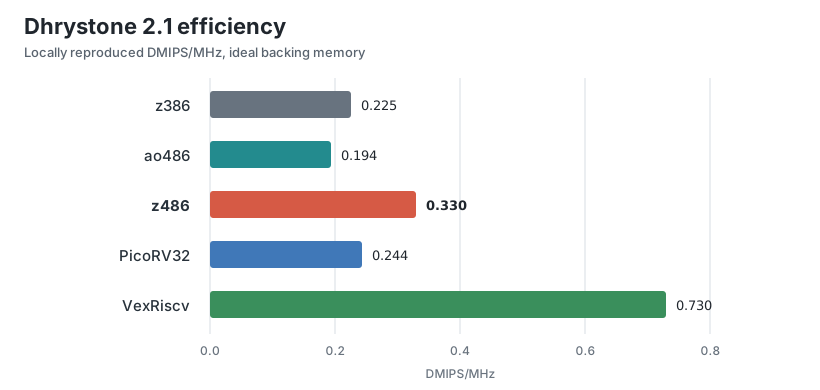
z486 uses 31.7% fewer cycles per iteration than z386 and 41.2% fewer than ao486. Its DMIPS/MHz is 46% above z386 and 70% above ao486. At the tested MiSTer clocks, the results are 28.05 DMIPS for z486 at 85 MHz, 19.15 for z386 at 85 MHz, and 17.46 for ao486 at 90 MHz. Source repositories, release clocks, and upstream results are listed in Further information and references.
Compiler and memory-interface choices have a large effect on Dhrystone scores. The local no-cache VexRiscv RV32IM build reaches 0.730 DMIPS/MHz, below the project's published 1.21 DMIPS/MHz for its full no-cache configuration and documented benchmark environment. PicoRV32 reaches 0.244 DMIPS/MHz locally; its project reports 0.516 with the look-ahead memory interface and 0.305 without it. The published configurations are linked in the final reference section.
CPI is derived from each binary's retired instruction count, so it should be compared across ISAs less precisely than cycles per iteration or DMIPS/MHz. The ao486 retirement event also occurs at a different pipeline boundary from the z386 and z486 event. These differences do not affect the measured cycle counts.
Doom: whole-system performance
Doom measures whole-system performance rather than isolated integer pipeline efficiency. Its timedemo exercises instruction decode and execution, caches, external memory, and video writes. All measurements use the same MiSTer setup at each core's release clock: 85 MHz for z386 and z486, and 90 MHz for ao486.
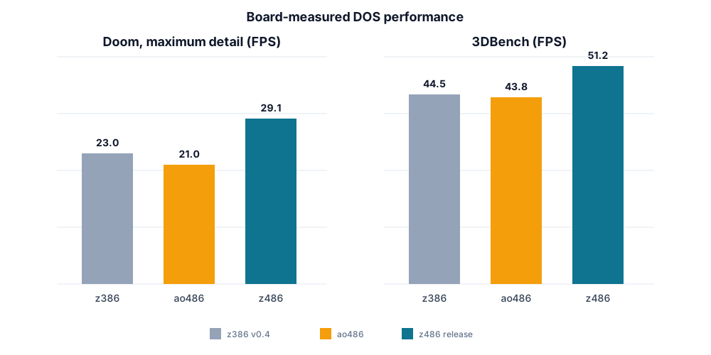
At maximum detail, z486 reaches 29.1 FPS in the Doom timedemo, 39% faster than ao486's 21.0 FPS and 27% faster than z386 v0.4's 23.0 FPS. The independent 3DBench result shows the same ordering. Doom represents complete DOS-system behavior; Dhrystone more directly isolates integer pipeline efficiency.
Verification
Verification for a pipelining CPU is harder than a sequential one as there is more parallelism. A value may belong to the wrong instruction, a fault may cancel EX while leaving a younger commit active, or a cache operation may race with a store or DMA snoop. Validation therefore covers both instruction semantics and inter-stage ordering.
The current validation stack includes:
- directed single-instruction tests;
- 9,410 real-mode and 1,220 protected-mode singlestep cases;
- protected-mode integration programs and the
test386suite; - focused instruction/data cache race tests;
- x87 command, stack, executor, TestFloat, and CPU integration tests;
- differential x87 traces against QEMU and a retired reference executor;
- deterministic Doom and Quake snapshots with RAM hashes;
- full-system DOS, Windows 3.1, Doom, Quake, demos, and game simulations; and
- five-seed Quartus comparisons followed by physical MiSTer testing.
Related work and future work
ao486 is the closest related open-source design and the CPU behind the established ao486 MiSTer core. It implements a 486SX-class integer processor with broad software compatibility, but no integrated x87. ao486 implements the 486 architecture directly; z486 instead evolved from a microcoded 386 core, adding a pipelined frontend, generated hardwired recipes for common instructions, and an application-focused x87. Because both run the same PC software on the same FPGA platform, their whole-system Doom results are more informative than area alone.
Open RISC-V cores cover a larger design space, from multi-cycle PicoRV32 to configurable pipelined VexRiscv. They provide useful Dhrystone and FPGA-efficiency reference points, but are not area-equivalent alternatives: the x86 cores also implement variable-length decode, segmented and paged protection, legacy execution modes, and a much larger compatibility surface.
Potential work includes:
- improving sustained cache-hit load throughput;
- reclaiming more redundant instruction-boundary slots through measured, timing-safe chaining;
- completing the remaining 486 and x87 instructions;
- moving x87 arithmetic toward the full 64-bit significand of the 80387;
- improving 85 MHz timing margin while retaining current CPI and area; and
- continuing compatibility work driven by DOS and Windows games and applications.
Conclusion
z486 shows that a microcode-driven 386 foundation can be extended into a practical pipelined FPGA CPU without replacing its complex architectural behavior with a large behavioral instruction engine. The D1/D2 frontend and generated hardwired recipes give common instructions i486-like timing, while the original microcode continues to handle protection, faults, task switching, and other irregular operations. A compact integrated x87 extends that approach to the floating-point subset needed by Quake.
The resulting core reaches 0.330 DMIPS/MHz and runs the maximum-detail Doom timedemo at 29.1 FPS on MiSTer, compared with 0.194 DMIPS/MHz and 21.0 FPS for ao486. It does so at 85 MHz in 35,686 of the DE10-Nano's 41,910 ALMs. The remaining two-cycle load latency, incomplete x87 instruction set, and limited timing margin also show where the FPGA implementation still differs from a complete i486-class processor.
Thanks for reading. You can follow me on X (@nand2mario) for updates, or use RSS.
Credits
z486 builds on the 80386 microcode disassembly and silicon reverse-engineering work of reenigne, gloriouscow, smartest blob, and Ken Shirriff. The i486 and 80387 analysis also draws on the Intel papers listed below. Thanks to the MiSTer community for extensive software testing and compatibility reports.
Further information and references
These notes collect the diagrams, historical sources, reverse-engineering work, benchmark configurations, and implementations discussed in this article.
-
Intel i486 functional block diagram. The diagram shows that the i486 pipeline comprises more than five abstract stage names. The register file, decoders, control ROM, address units, TLB, cache, execution units, and internal buses were arranged to overlap decode, address generation, translation, and execution. That organization is the main architectural reference for z486's integer pipeline.
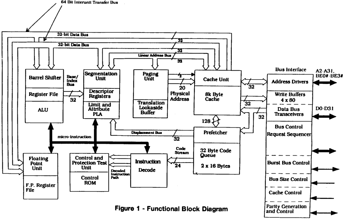 Intel i486 functional block diagram. Click for the full image. Source: Fu, Saini, and Gelsinger, Performance and Microarchitecture of the i486 Processor, Figure 1; reference 5 below.
 -
Intel 80387 block diagram. The 80387 drawing exposes the boundaries hidden by the x87 instruction set: bus control, command sequencing, the register stack, exponent logic, mantissa datapath, barrel shifter, and CORDIC engine. z486 preserves the broad control/datapath split while mapping storage and arithmetic onto FPGA block RAM and DSP resources.
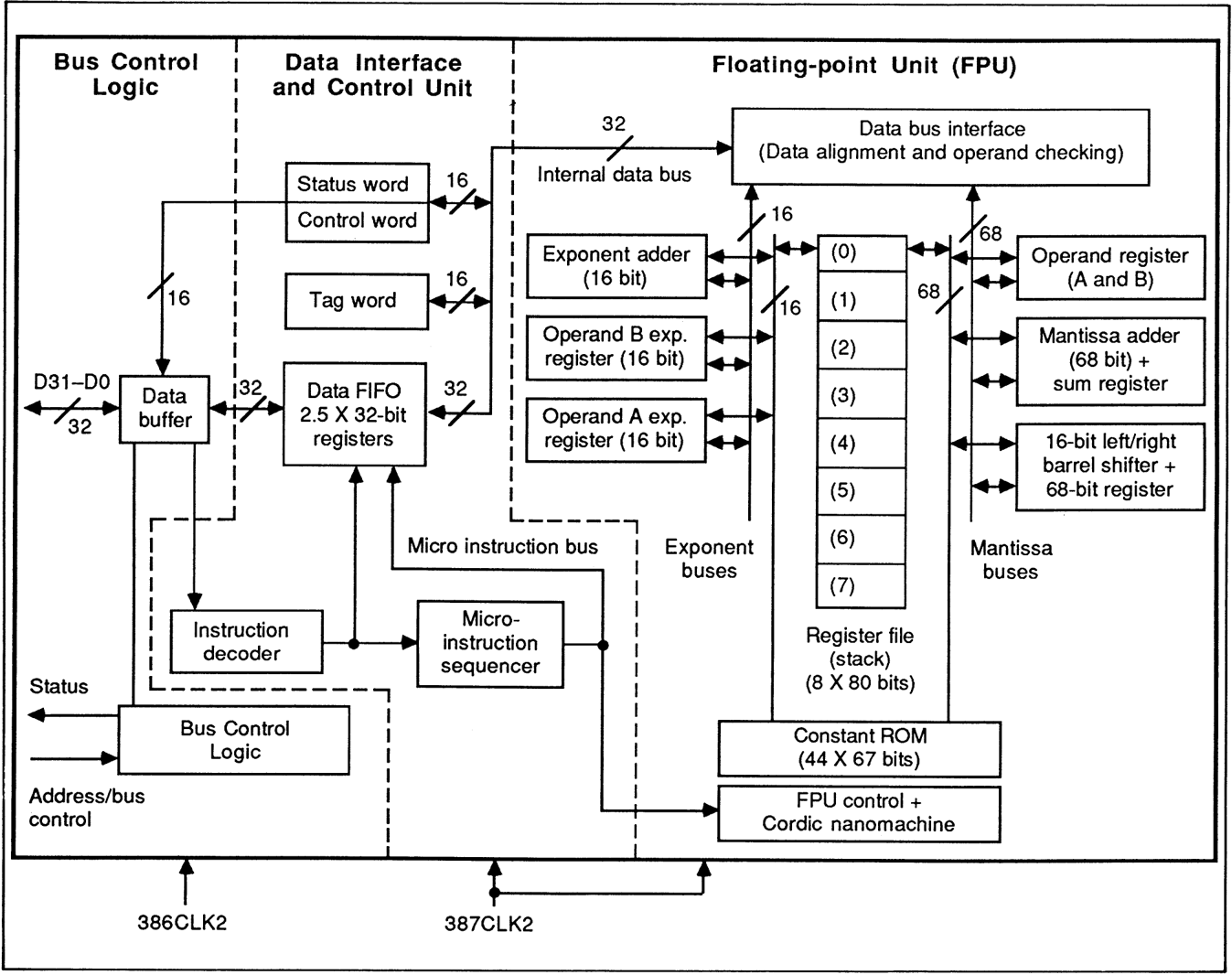 Intel 80387 block diagram. Click for the full image. Source: Perlmutter and Yuen, The 80387 and Its Applications, Figure 2; reference 6 below.
 -
John H. Crawford, “The i486 CPU: Executing Instructions in One Clock Cycle”, IEEE Micro, 1990. This describes the five-stage pipeline, hardwired instructions, D1/D2 split, and one-cycle execution target.
- John H. Crawford, “The Execution Pipeline of the Intel i486 CPU”, Compcon Spring, 1990. This gives a complementary description of pipeline timing and interlocks.
- B. Fu, A. Saini, and P. Gelsinger, “Performance and Microarchitecture of the i486 Processor,” ICCD, 1989. The i486 block diagram in note 1 is Figure 1 of this paper.
- David Perlmutter and Alan Kin-Wah Yuen, “The 80387 and Its Applications,” IEEE Micro, 1987. The 80387 block diagram in note 2 is Figure 2 of this paper.
- John F. Palmer, “The Intel 8087 Numeric Data Processor”, 1980. This describes the stack architecture and the original numeric-coprocessor organization inherited by later x87 designs.
- reenigne, “80386 microcode disassembled”. Its extraction and disassembly work made the original z386 microcode-driven control path possible.
- The PicoRV32 evaluation notes document the upstream Dhrystone configurations and published scores cited for comparison.
- The VexRiscv area and frequency results document its published Dhrystone and implementation configurations.
- The ao486_MiSTer documentation records its core clock and system configuration. Its Dhrystone and Doom results in this article were reproduced locally.
- The z386 repository contains the earlier 80386-oriented core used as the architectural and performance baseline.
- The z486 repository contains the CPU RTL, tests, design documentation, and reproducible Dhrystone evaluation framework.
- The z486_MiSTer repository contains the complete MiSTer system, while the 20260813 release records the 85 MHz release configuration evaluated here.
Comments