The Pentium Pro (P6) translates complex x86 instructions into simpler, RISC-like micro-operations (µops), executes them out of order, and retires them in program order. That combination made it a much more complex machine than the 486 or original Pentium. The basic P6 pattern, including µop translation, register renaming, out-of-order scheduling, and in-order retirement, continues in many later Intel cores till today.
This page follows those µops through the P6's overlapping pipelines, from fetching instruction bytes to committing results. The two main sources are Shen and Lipasti's Modern Processor Design, Chapter 7 and Intel's P6-era patents. The book gives the overall organization; the patents add module interfaces and stage timing.
P6 has several concurrent pipelines. Its in-order front end feeds a queue; the rename and allocation stages place µops into the reservation station and reorder buffer. Execution, memory and result writeback overlap, while retirement commits results in program order. Queues and result buses connect these paths.
- Reading the pipeline diagrams
- Pipeline stages at a glance
- The whole pipeline
- 11 NextIP
- 12 ICache1 (and BTB start)
- 13 ICache2/ILD (and BTB complete)
- 14 ICache3/Rotate (and write the IFBR)
- 15 ID0 — steer, XLAT, start MSROM
- 16 ID1 — alias mux and ID output queue
- 17 Branch decode
- 20 Exit ID queue
- 21 RAT / ALLOC / RS1 / ROB1
- 22 ROB read / RS2
- 31–32 — reservation-station schedule and dispatch
- 33 and later — execution
- 40–43 — memory and blocked-load retry
- 81–83 — result-bus scheduling and writeback
- 91–93 — in-order retirement
- References and figure credits
The stage numbers group 1x work around fetch/decode, 2x around rename/allocation and 3x around dispatch/execution.
For a quick visual tour of the P6 chip, and its various blocks (RS, ROB, RAT, and ...), see P6 ROMs and PLAs.
Reading the pipeline diagrams
| Source | Content |
|---|---|
| Chapter 7 §7.2.1 / Fig. 7.4 | Whole machine, pipeline overview |
| US5721855 Fig. 5, 9–11, 13, 15, 17a | IFU 11–14, ID 15–16 (and ID-side 17H/17L immediates), BAC 14–17, RAT/RS/ROB 21–22 |
| Chapter 7 §§7.2.2–7.2.3, 7.4–7.5 | RS 31–32, execution 33+, memory 40–43, writeback 81–83, retirement 91–93 |
| US5721855 Figs. 14–17c, 23–24, 29–30 | RS, execution, ROB writeback, AGU/DCU/MOB and retirement half-cycle detail |
| US5559974 | What 15/16 compute (Cuop + aliases → Auop) |
| US5630083 | ILD marks and steering into 15 |
| US5673427 Fig. 6 | Main/shadow queues, immediate bypass and post-queue integer constant ROM |
Pipeline stages at a glance
The main blocks are the instruction fetch unit (IFU), instruction decoder (ID), register alias table (RAT), reservation station (RS), reorder buffer (ROB), real register file (RRF), and memory ordering buffer (MOB). The branch target buffer (BTB) and branch address calculator (BAC) steer fetch before a branch reaches an execution unit. Other names appear with their diagrams below.
| Stage | Name | Work |
|---|---|---|
| 11 | NextIP | Pick the linear fetch address from sequential, BTB, BAC, JEU |
| 12 | ICache1 (and BTB start) | Start I-cache, ISB, IVC, ITLB, and the two-cycle BTB |
| 13 | ICache2/ILD (and BTB complete) | Continue cache read; mark instruction boundaries; receive BTB prediction |
| 14 | ICache3/Rotate (and write the IFBR) | Rotate a 16-byte marked window into the ID input buffer |
| 15 | ID0 — steer, XLAT, start MSROM | Steer bytes; XLAT PLA emits Cuops; field extractor supplies MAR fields |
| 16 | ID1 — alias mux and ID output queue | Resolve aliases into Auops and enqueue them |
| 17 | Branch decode | BAC validation, static prediction and RSB write; aligns with 21 |
| 20 | Exit ID queue | Dequeue up to three µops toward RAT/ALLOC (Chapter 7 Fig. 7.4 only) |
| 21 | RAT / ALLOC / RS1 / ROB1 | Rename, allocate ROB/RS/MOB, write RS PSrc/control (21L) |
| 22 | ROB read / RS2 | Read ROB/RRF sources; write RS data (22L); in-order → OoO |
| 31–32 | reservation-station schedule and dispatch | Select ready µops (31H/31L), then read/bypass operands and dispatch (32H/32L) |
| 33 and later | execution | Execute simple integer and AGU work; multicycle operations continue |
| 40–43 | memory and blocked-load retry | Wake and re-dispatch blocked loads (40–41); access DTLB and DCU (42–43) |
| 81–83 | result-bus scheduling and writeback | Arbitrate result buses (81–82); broadcast PDst, data, flags or events (83) |
| 91–93 | in-order retirement | Feed back the pointer (91), read/qualify oldest entries (92), then handle events/IP and write RRF (93) |
The whole pipeline
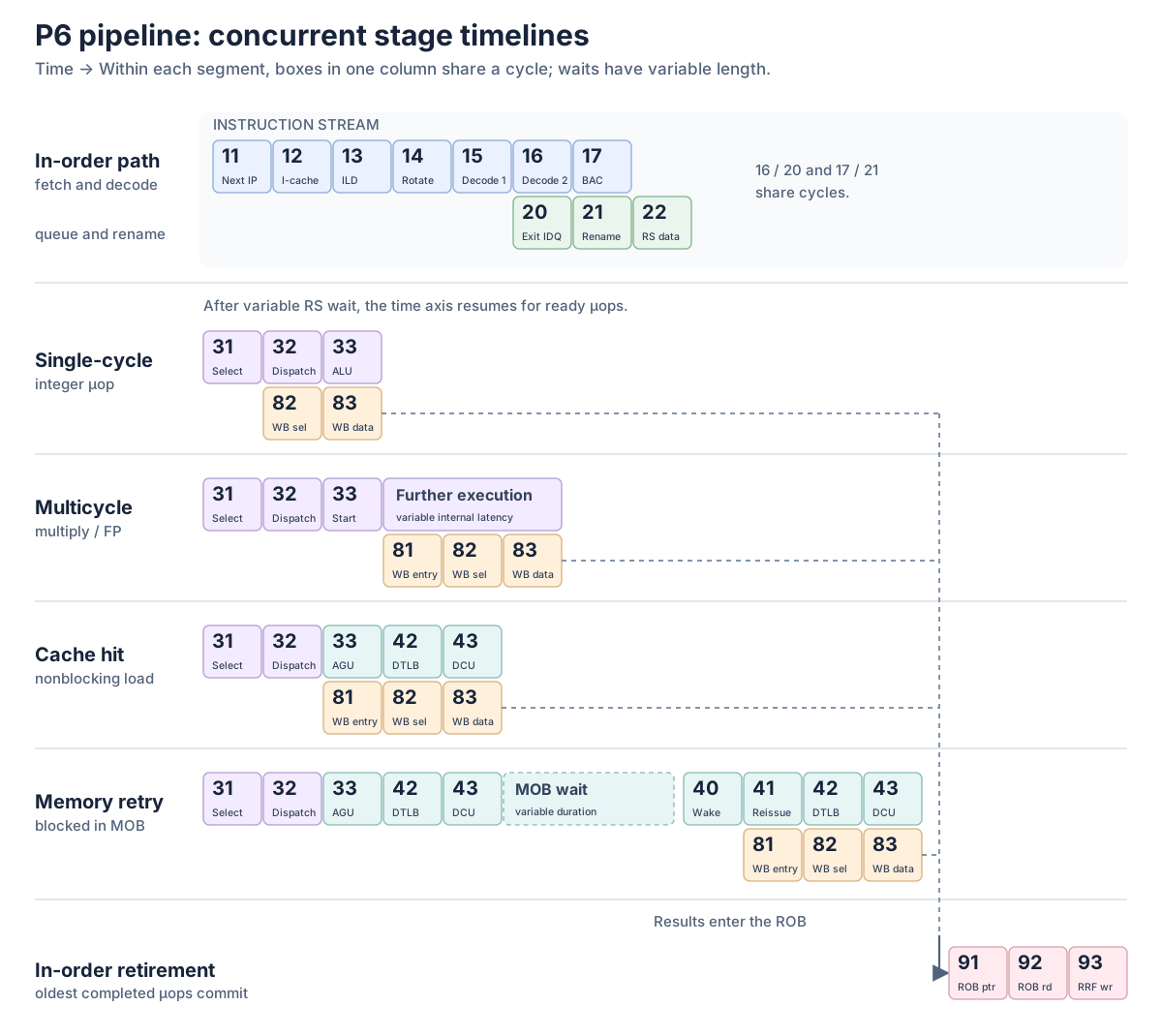
Fetch, decode and rename proceed in order. The reservation station can hold a µop while its operands or execution port are unavailable; memory operations may also wait or retry. Writeback supplies the ROB, while retirement commits completed work in program order. These paths overlap rather than following a single fixed-length sequence.
11 NextIP
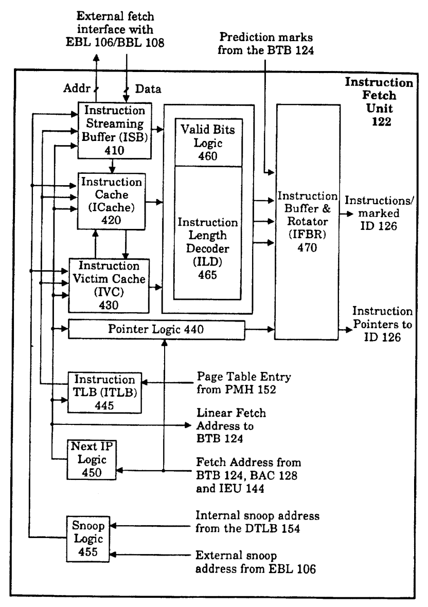
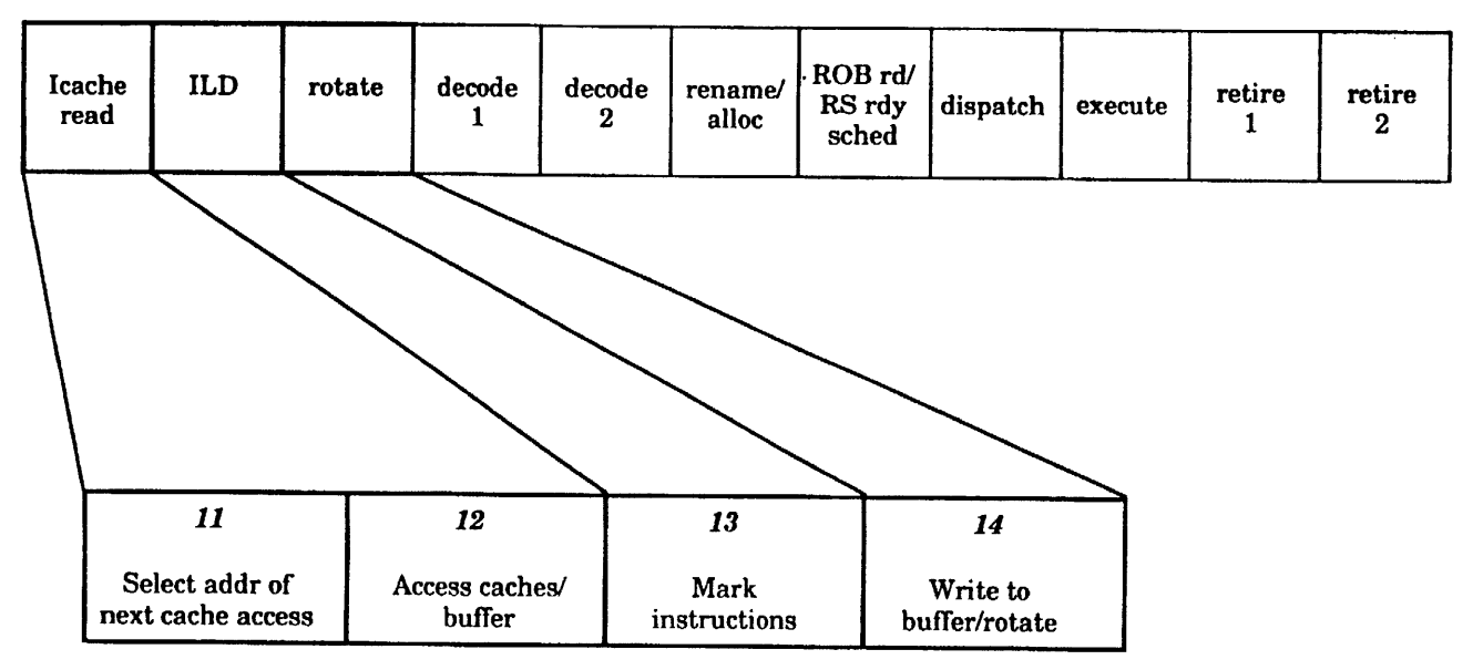
The IFU selects the linear address of the next cache access from competing requests: sequential IP, a previous BTB prediction, a BAC correction, or a JEU redirect (US5721855 Fig. 5; Chapter 7 §7.2.1 / §7.3.1). It schedules that request for service in 12.
12 ICache1 (and BTB start)
The IFU uses the stage-11 address to access ISB, I-cache and IVC. In parallel the ITLB translates linear→physical and reads the memory type, and the BTB starts its access (US5721855 Fig. 5 text: pipestage 12 accesses the 32-byte Instruction Streaming Buffer (ISB)/I-cache/IVC and the BTB). A miss in all instruction buffers starts an external fetch.
The BTB takes two clocks. Prediction status and target arrive by the end of 13, after the lookup starts in 12 (Chapter 7 §7.3.2).
13 ICache2/ILD (and BTB complete)
I-cache/buffer read continues. The ILD marks instruction boundaries (start, end, invalid bytes, prefixes) on the bytes from 12. Predicted-branch marks from the BTB are attached here and travel with the line into the IFBR (US5721855 Fig. 5: pipestage 13 is “mark instructions”; Chapter 7 §7.3.1: marks plus BTB prediction marks by the end of 13). Speculative BTB history update is the stage-13 BTB side (Chapter 7 §7.3.2).
The ILD marks first opcode and last byte positions ahead of the three decoders, so steering need not discover all three variable-length boundaries serially in stage 15. A predicted branch is attached to its last-byte mark, which also lets ID check that the BTB's target belongs to a real instruction boundary. See Chapter 7 §7.3.3 and US5630083.
14 ICache3/Rotate (and write the IFBR)
The fetched bytes and marks pass through the IFU buffer and rotator as an instruction-aligned 16-byte window offered to the ID (Instruction Buffer & Rotator (IFBR)) when it has space (US5721855 Fig. 5; Chapter 7 §7.3.1).
The buffer retains the stream while ID takes several clocks to consume its complete instructions. On a predicted-taken branch, ID can grab the target's fetched block before it decodes the branch, keeping that block ready for the rotator when the branch finally reaches a decoder. This is a separate timing path from the sequential stream; it prevents a late target request from turning every predicted branch into a fetch bubble (Chapter 7 §7.3.3.2).
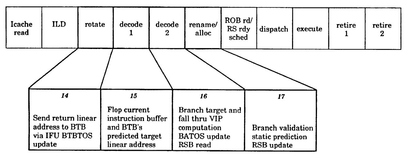
BAC work in 14 is only the BTB-detected call/return assist: send the RSB return linear address to the BTB and update a TOS pointer (US5721855 Fig. 11a). The RSB read for decoded CALL/RET is 16; the RSB write is 17. 14 is not the full return-stack lookup.
15 ID0 — steer, XLAT, start MSROM
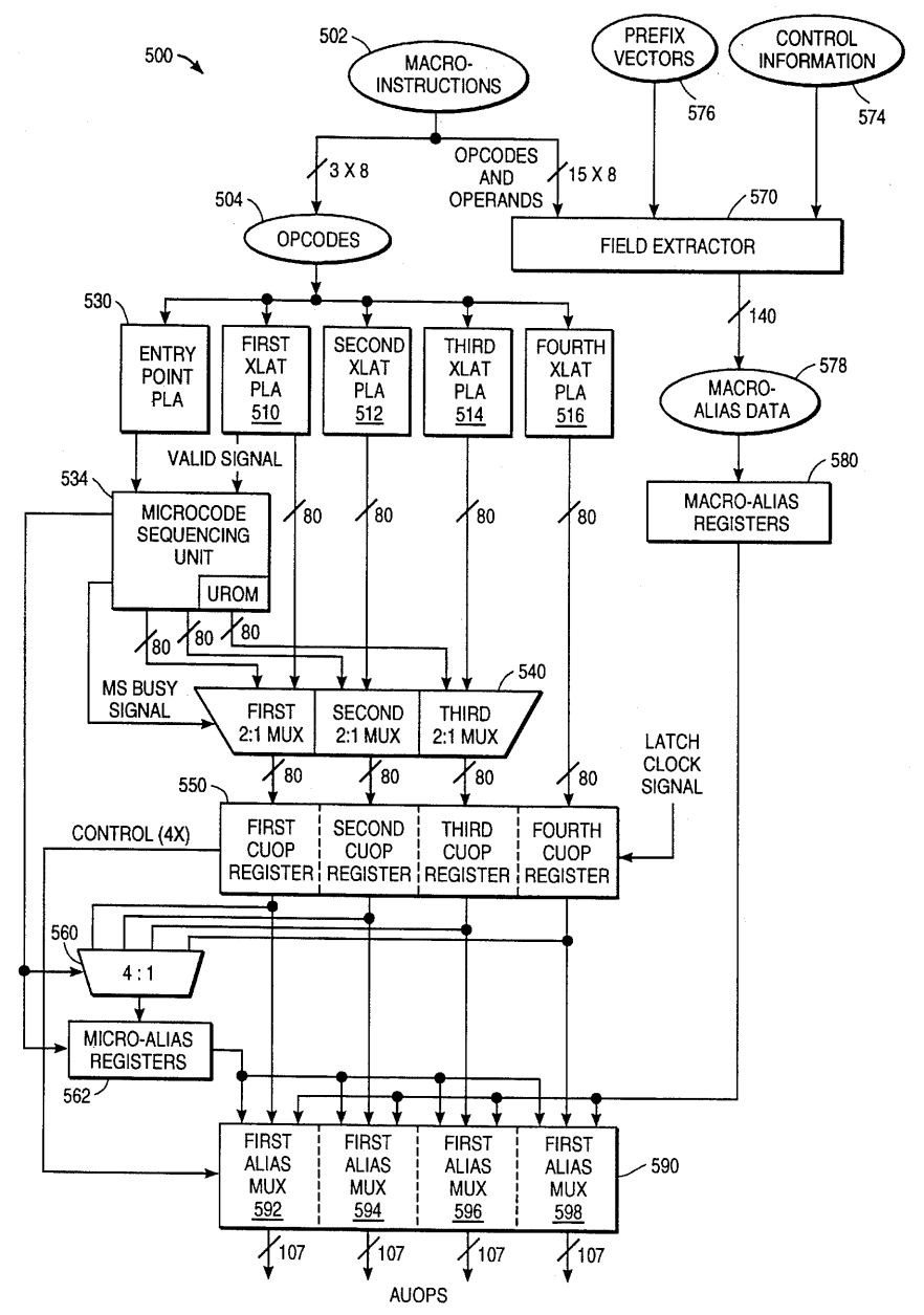
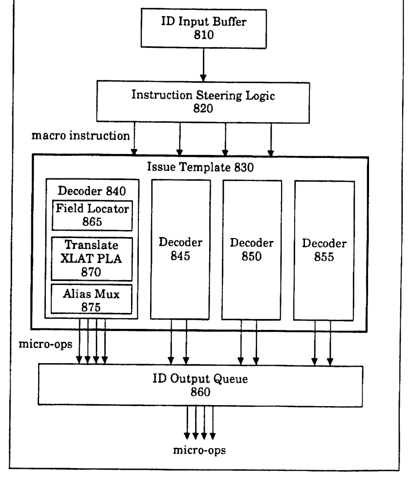
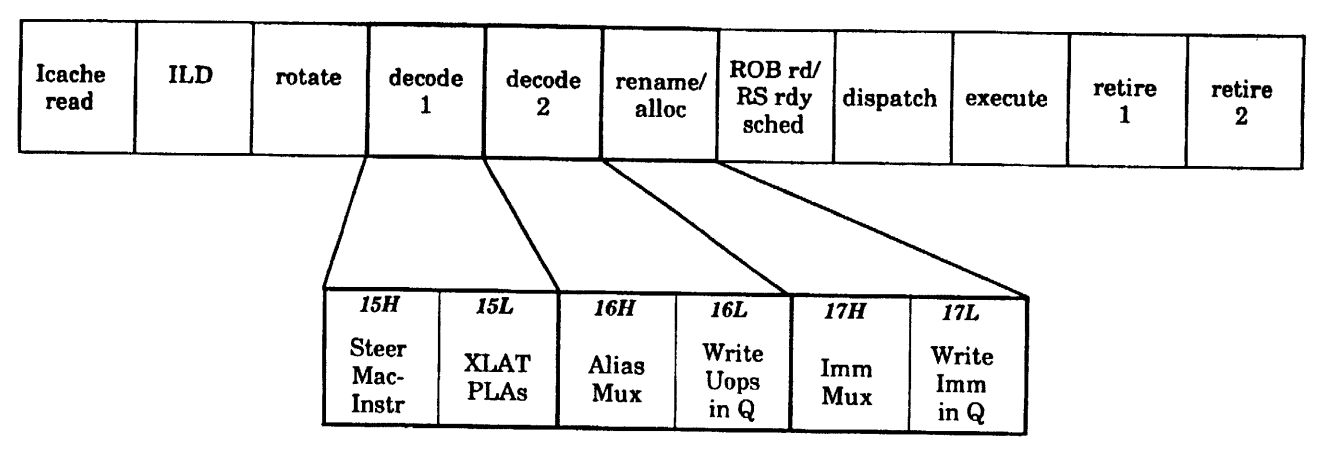
Marked bytes in the ID input buffer (IFBR) are aligned and steered to decoder 0 and the simple decoders. Fig. 9 splits the clock: 15H steer the macroinstruction; 15L XLAT PLAs emit Cuop templates while field locators write immediates, displacements and register fields into the macro-alias registers (US5721855 Fig. 9; US5559974).
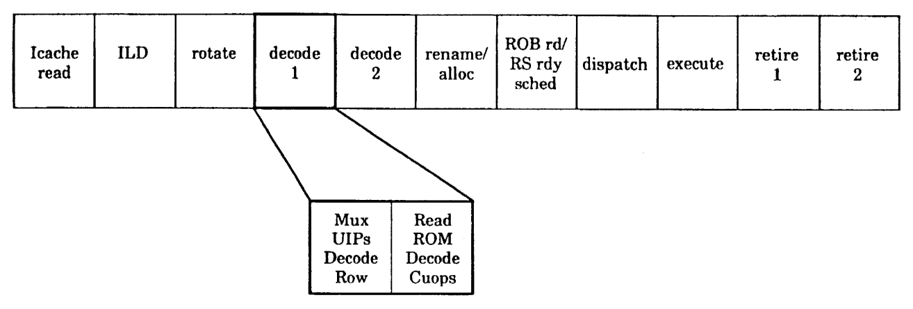
MSROM is summoned in this first decode pipestage: form the micro-IP, start the UROM read, and decode the previous triad’s sequencing for the next clock (US5721855 Fig. 10).
US5559974 Fig. 5 adds the decoder-0 wiring that the stage diagram omits. Opcode bits address four XLAT PLAs and an entry-point PLA in parallel. The entry PLA can start the microcode sequencer; three Cuop lanes then select XLAT or UROM output, while the fourth comes from XLAT. Separately, the field extractor decodes the instruction bytes, prefixes and mode bits into macro-alias registers (MAR). This separation explains why reading a Cuop template alone does not supply its final register numbers, displacement or immediate value. The figure is a patent embodiment; it does not itself reveal the contents of a particular chip's XLAT or entry-point PLA.
BAC in 15 only latches the current instruction buffer and the BTB’s predicted target (Fig. 11a).
16 ID1 — alias mux and ID output queue
Alias multiplexers merge Cuops (XLAT or MS) with MAR/UAR fields to form Auops. Those Auops are written into the ID output queue, which decouples decode from rename (US5721855 Fig. 9: 16H alias mux, 16L write µops in Q; Chapter 7 Fig. 7.10 six-entry queue). Fig. 5 of US5559974 also shows the micro-alias registers (UAR) taking selected Cuop register fields and feeding them back into later alias muxes. MAR is instruction-derived; UAR is microcode-flow-derived. This is a control/data path through the decoder, not an extra scheduled execution µop.
Fig. 9 also shows 17H/17L immediate mux/write into the same queue. That is ID-side pipe 17 on the decode segment, concurrent with BAC 17 and rename 21.
BAC in 16 computes branch and fall-through VIP and reads the RSB (Fig. 11a).
17 Branch decode
The BAC inspects the decoded instruction: validate the BTB, static-predict an unpredicted branch, write the RSB (Fig. 11a). On a BAC-detected mispredict it flushes the in-order front end (11–16) and redirects IFU, without waiting for JEU/retirement (Chapter 7 §7.2.1).
Stage 17 on the decode segment lines up with stage 21 on the rename segment. It is not an additional decode pipeline stage.
20 Exit ID queue
Figure 7.4 labels 20: Exit ID queue. Up to three µops per clock leave the six-entry queue toward RAT/ALLOC. US5721855 does not label a stage 20: its Figure 9 shows queue writes in 16L–17L, and Figures 15 and 17a resume at 21H. Stage 20 names that hand-off, rather than another registered ID stage.
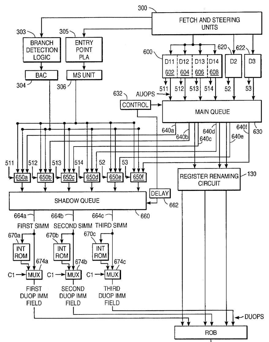
The Auop control and its immediate/displacement payload take parallel paths across this handoff. US5673427 Fig. 6 shows the main queue sending up to three Auops into renaming, while a shadow queue carries their 32-bit immediate candidates one clock later. Both queues use corresponding slot controls; a stall must hold them together. The immediate path can select a small Cuop literal, a MAR immediate or displacement, a macro-branch address or a micro-branch address. At the shadow queue output, an integer constant-ROM index can be expanded and selected in place of the literal. This places only three constant-ROM read paths after the queue instead of six before it. Renamed control and resolved immediates meet as the µop enters the out-of-order core; the RAT does not rename constants. The patent's queue widths and timing are a published embodiment, not proof that the raw Cuop immediate field is itself a full 32-bit value.
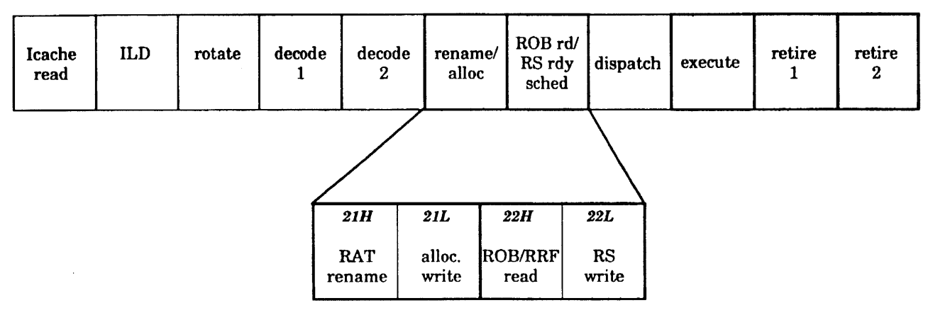
21 RAT / ALLOC / RS1 / ROB1
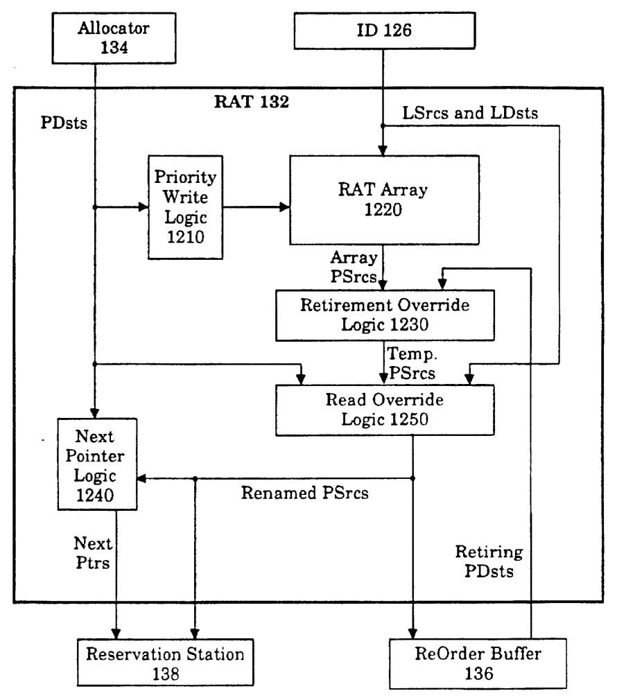
The RAT maps logical sources/destinations to ROB PSrc/PDst. The allocator
grants ROB entries and RS (and MOB) slots. Control and PDst tags are written
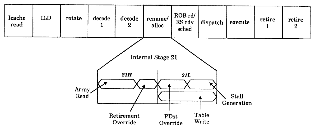
into those entries — Fig. 15 21L RS write PSrcs, Fig. 17a 21L alloc write,
Fig. 13 21H array read / retirement override then 21L table write.
An RAT entry distinguishes a speculative ROB source from a committed
RRF source with its RRF-valid selector. In the same three-µop rename group,
comparators override a table read with the nearest older lane's newly
allocated PDst when logical names match. Retirement can restore an RRF
mapping only if no younger writer now owns that name. The allocator gives
each µop a sequential ROB slot; its PDst becomes that µop's name through
RS, execution, result broadcast and retirement. See
Chapter 7 §7.3.4
and US5721855 Figs. 12–13.
22 ROB read / RS2
PSrcs from 21 read committed data from the RRF or speculative data from the
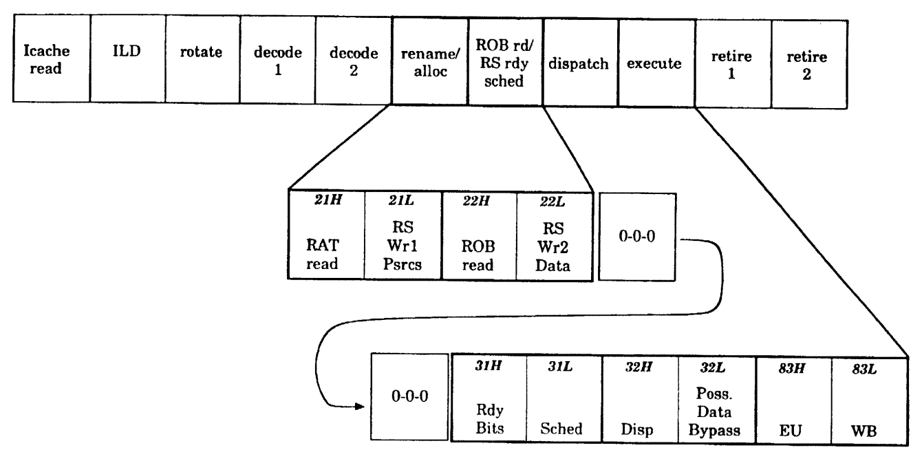
ROB. Values and ready bits are written into the RS (22L). Fig. 15: 22H ROB
read, 22L RS write data. Fig. 17a: 22H ROB/RRF read, 22L RS write.
The RS entry already has its source identities and control from 21L; 22L
installs values that are available now. An incomplete ROB source leaves its
identity resident so a later matching PDst writeback can fill it. A coincident
writeback may supply the value by bypass instead of waiting for the array
read. The ROB entry itself holds retirement metadata written at allocation;
the RS need not carry every field required only at retirement.
After 22 the µop is in the RS and has a ROB row: the in-order → out-of-order boundary (Chapter 7 §7.2.1; Fig. 7.4).
31–32 — reservation-station schedule and dispatch
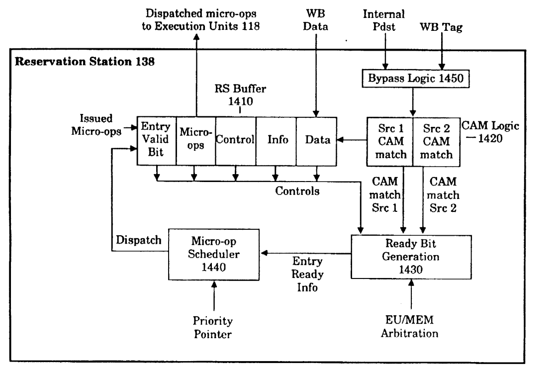
After stage 22, µops wait in the RS until their operands and execution resources are ready. Chapter 7 §7.4.1 describes a 20-entry RS whose control arrives from allocation/RAT and whose source data arrive from ROB/RRF reads or matching result broadcasts. Its five dispatch interfaces are two execution-unit ports, two AGU ports and one store data port. Fig. 7.14 shows the port-to-unit mapping and bypass paths; a port is an interface, not a promise that five arbitrary µops can execute together.
In 31, source-valid CAM matches, unit availability, writeback capacity and
scheduling priority determine candidates. The patent places ready-bit work in
31H and scheduling in 31L. In 32, selected entries and operands are read,
late data may bypass the RS array, and the operations are dispatched. A row is
released after successful, uncanceled dispatch. The RS may predict the arrival
of load data early enough to schedule a dependent µop; if the load misses, the
dependent dispatch must be canceled and later retried. Thus 31–32 describe
work after a potentially long RS wait, not two clocks after every stage-22
insertion. US5721855 Fig. 14 makes the
hardware path explicit: each stored PSrc compares against broadcast PDst in a
CAM; matches drive operand capture or bypass. The entry-valid bit, operation,
controls, matches and unit arbitration produce a ready bit. The scheduler uses
ready bits and a priority pointer to select entries. Fig. 15 above locates
source installation and schedule/dispatch half-stages. See the
patent description.
33 and later — execution
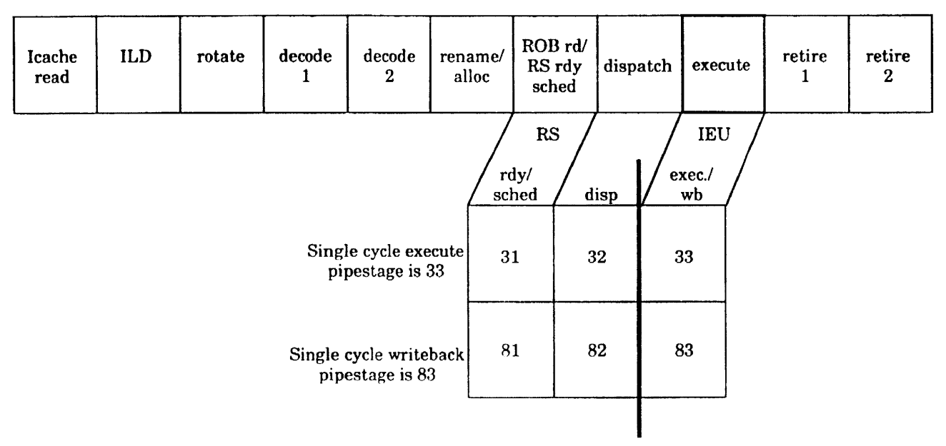
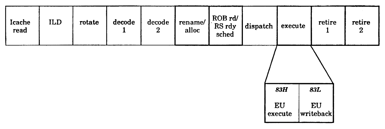
A simple integer µop executes in 33; its result is ready for writeback at
the end of that stage. The IEU's patent drawing aligns execution 83H and
writeback 83L with this same clock, rather than adding a separate universal
writeback clock. Multiply, divide and floating-point operations start from the
same RS dispatch but take further execution cycles before their result reaches
the writeback pipeline. See Chapter 7 §7.2.2,
US5721855 Fig. 17b
and Fig. 23.
Fig. 23 shows the IEU interface explicitly: µop, operands, flags and PDst
arrive from the RS in 32; result data, flags and fault information return on
the writeback paths in 33/83.
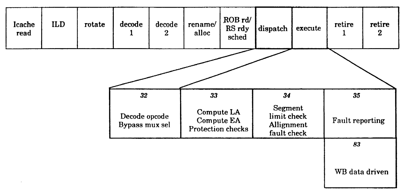
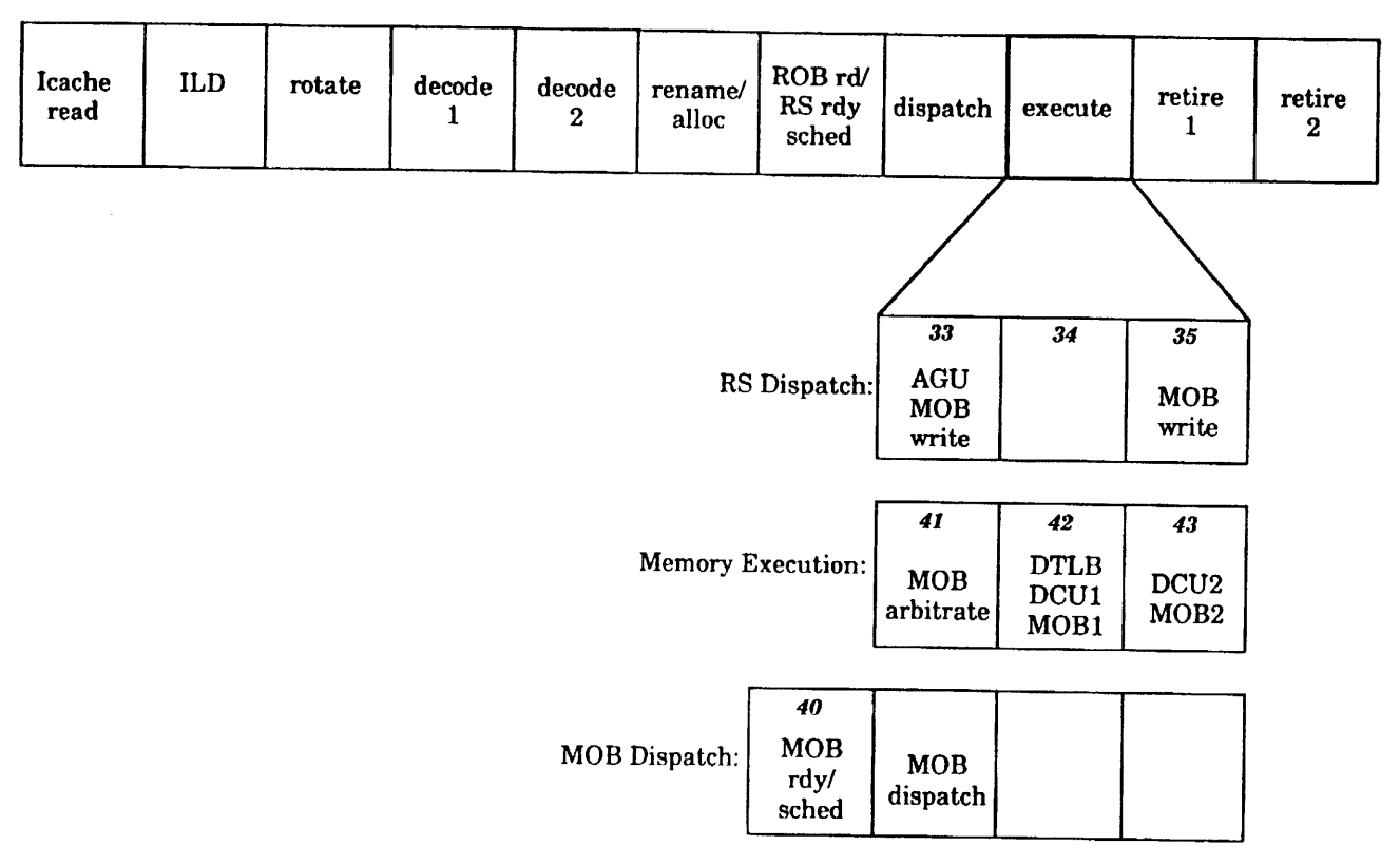
For a memory µop, the AGU forms the linear address in 33 from the effective-address operands and segment state. The DTLB, DCU and MOB then own translation, cache access and ordering. Store address (STA) and store data (STD) arrive on different RS interfaces and meet in the store buffers; they are not an immediate architectural memory write. The AGU's stage-33 calculation overlaps the start of the memory path, as shown in US5721855 Fig. 24a. The patent splits AGU work further: stage 32 opcode/bypass selection, 33 linear/effective-address and protection calculation, 34 segment-limit and alignment checks, and 35 fault reporting, aligned with memory 41–43. These are overlapping pipelines, not three extra clocks before a cache hit.
40–43 — memory and blocked-load retry
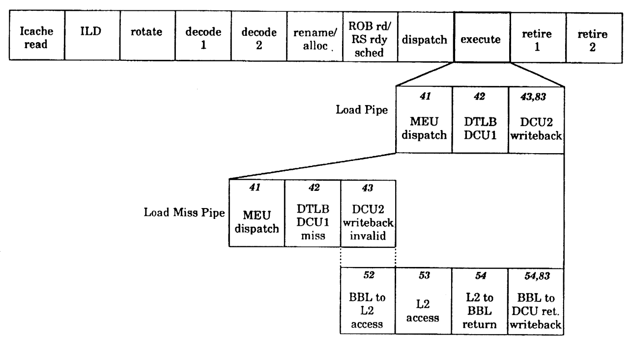
On an unblocked load, the MOB bypasses its wait queue into the DCU path. The AGU produces the address in 33; the DTLB translates and the DCU begins its lookup in 42, with data returned on a hit in 43. The patent additionally labels 41 as DCU dispatch: its memory 41–43 path overlaps the AGU 33–35 path, rather than following all three AGU clocks. It describes a parallel low-address tag read and DTLB translation in 42, then physical tag comparison and data return. Chapter 7 Fig. 7.4 compresses this hit path to 33→42→43; US5721855 Fig. 29 gives the finer stage-41 view.
On a miss or ordering/resource block, the MOB retains the load. 40 wakes and schedules a blocked entry, 41 re-dispatches it, and 42–43 retry the cache access. The interval before 40 is variable; it can include an L2/memory fill or a store conflict. This is the separate nonblocking memory loop in Fig. 7.4, not a fixed penalty applied to every load. The MOB also tracks stores, but they become architecturally committed only at retirement; then it can send senior store data to the cache in program order. See Chapter 7 §§7.2.2, 7.6 and US5721855 Fig. 30.
Fig. 29 shows the cache-hit, miss, L2-return and store-dispatch paths on one sheet. Fig. 30 shows why a blocked load does not occupy the RS until memory responds: the MOB can schedule it again from its own buffer. A store's buffer ownership continues after its STA/STD µops retire until the senior store is actually sent to the DCU.
81–83 — result-bus scheduling and writeback
The 81/82 labels in Fig. 7.4 distinguish the scheduling/arbitration of memory/FP and integer result paths. They overlap the tail of execution; they are not three additional clocks appended to every µop. 83 is the actual result-data writeback. A result carries its physical destination (PDst), data, and any flags or event information to the ROB; matching RS sources capture or bypass the broadcast. A load hit can use the memory writeback path after 43, while a simple integer result writes back during its stage 33/83 clock.
The RS must reserve a suitable writeback bus when it schedules work whose completion time is known. A miss or cancellation can invalidate a predicted result arrival, requiring the dependent wakeup/dispatch to be canceled. Chapter 7 §§7.2.2, 7.4.1 and US5721855 Fig. 17b describe the separation of RS scheduling, EU execution and ROB result write. This is speculative completion: the RRF and architectural memory state have not yet been updated.
91–93 — in-order retirement
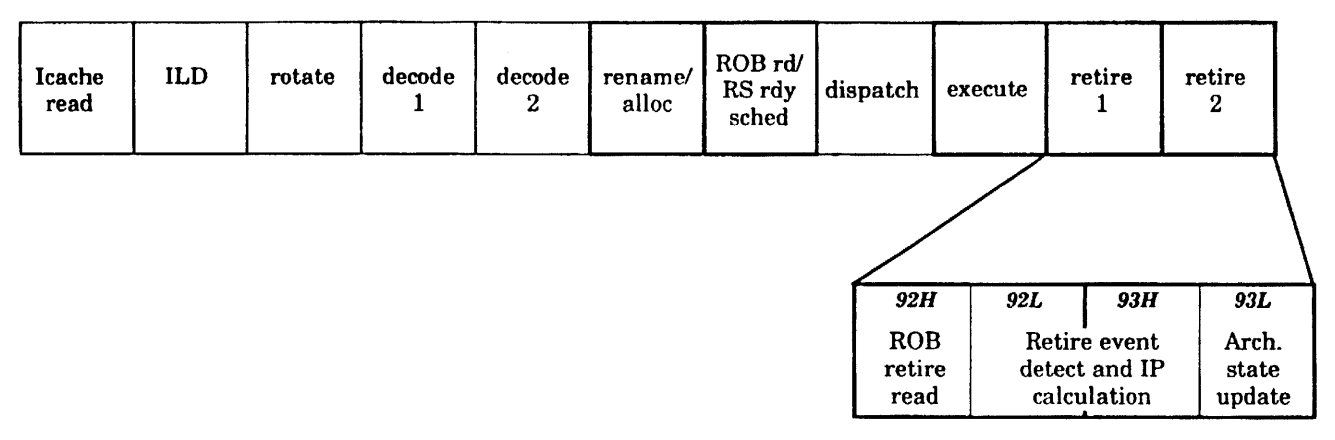
The ROB stores results under their PDst and retains the original order of
allocated µops. Its retirement pointer visits the oldest entries, regardless
of the order in which execution finished. The 91 label in Chapter 7 Fig. 7.4 is
retirement-pointer write/feedback. The chapter explicitly calls retirement
a two-clock operation in 92 and 93; treating 91 as an obligatory extra
candidate-processing stage would misread that diagram.
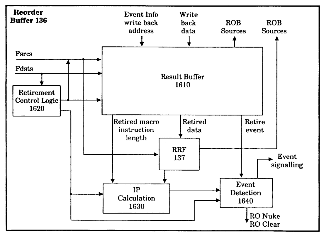
The patent's Fig. 16 separates the ROB result buffer, retirement
control, IP calculation, event detection and committed RRF.
That separation explains why result writeback can proceed out of order while
architectural register and IP updates remain ordered.
In 92H, the retirement control reads candidates from the ROB; in 92L, it decides which oldest, consecutively ready candidates can retire. In 93H, event detection and instruction-pointer calculation process that ordered set; in 93L, eligible values transfer to the RRF. At most three µops retire per clock in the chapter's P6 description. First/last marks from the decoder preserve the architectural boundary of an x86 instruction: interrupts and faults cannot expose a partially committed instruction. The patent's generic example discusses four physical-register candidates, so its example width should not replace the chapter's three-µop P6 width. See Chapter 7 §§7.2.3, 7.5.1.1 and US5721855 Fig. 16–17c.
The ROB also arbitrates recovery. A jump-unit misprediction can clear and redirect the in-order frontend early; the ROB still prevents younger wrong-path state from retiring, and a retirement clear repairs the out-of-order state. A faulting µop's event is carried with its speculative result and handled when it reaches the ordered retirement boundary. Senior stores leave the ROB's speculative domain only on retirement and may complete at the DCU later. These recovery, event and store paths are distinct from ordinary 83 writeback; see Chapter 7 §§7.2.3, 7.5.1, 7.6 and US5721855 ROB description.
References and figure credits
- John Paul Shen and Mikko H. Lipasti, Modern Processor Design, Chapter 7, especially Figures 7.4, 7.6, 7.10 and 7.14 (cited for technical detail; book figures are not reproduced here).
- US5721855, pipeline, execution, memory and ROB figures.
- US5559974, decoder aliases and microcode sequencing, Figure 5.
- US5630083, parallel instruction decoding.
- US5673427, main and shadow µop queues, Figure 6.