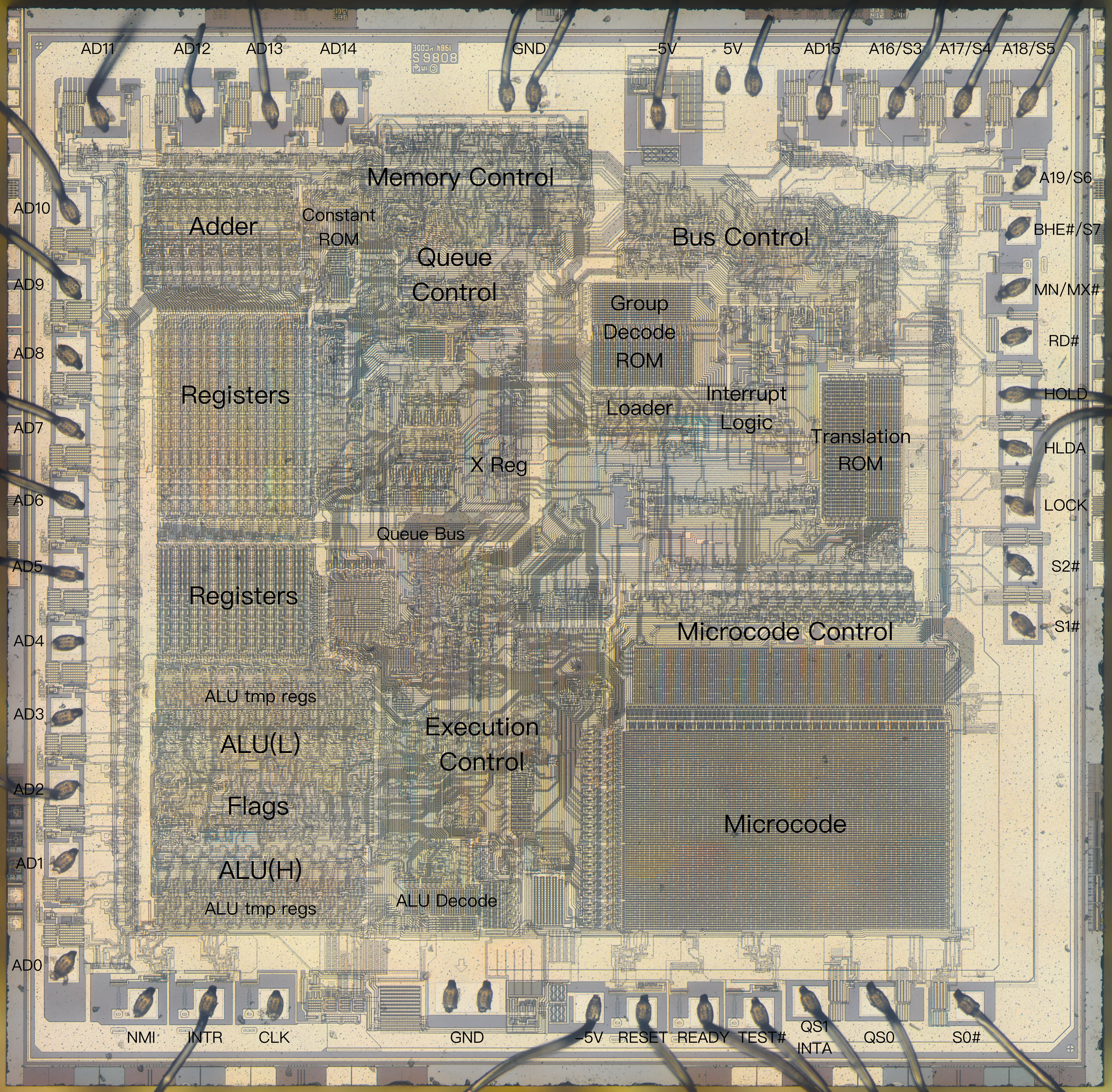
8086-S die shot with labeled functional blocks
You can view the full-resolution image (12780x12554, 62MB) at https://github.com/nand2mario/dieshots/blob/main/intel-8086/8086s_metal.jpg.
This is a die shot of the 8086-S chip that I captured in November 2025. The 8086-S is a revision and die shrink of the original 8086, manufactured with 3 µm HMOS II (a form of NMOS). I photographed it using my Canon camera mounted on an old Olympus BH2-UMA microscope, equipped with a budget MSPLAN ULW 20X objective. To cover the entire die, I took around 250 photos, manually moving the microscope stage and overlapping each shot by about one third. I then used the open-source Hugin software to stitch them together, aided by some SIFT-based Python scripts I wrote. These scripts sped up the process by leveraging the grid-like layout of the photos, since standard Hugin can be slow at matching each pair of images.
After assembling the image, I added labels for the functional blocks and pin names. The 8086 was entirely manually laid out, so its functional block boundaries are quite regular.